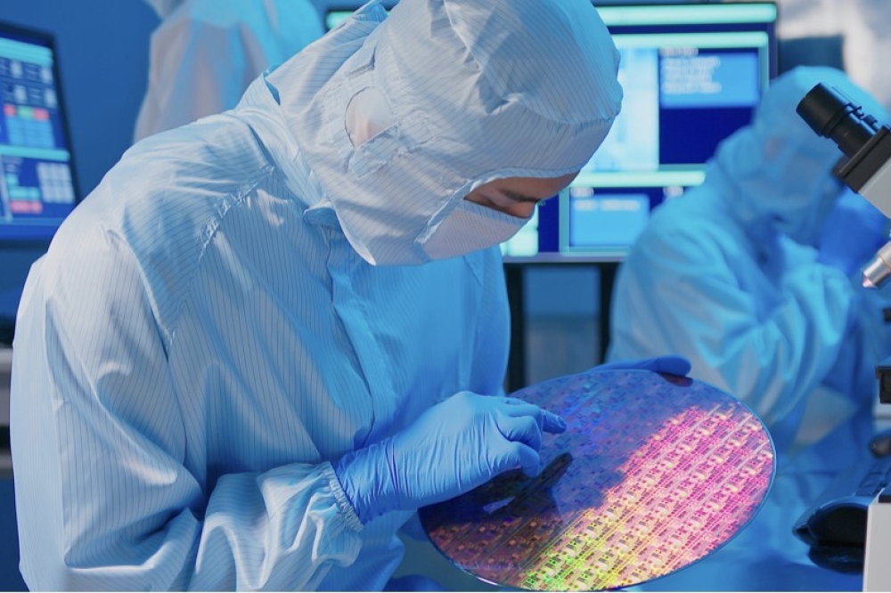
GaN VCSELs: Refining the production process
Superior control of the cavity thickness enhances the capability to target an emission wavelength
Engineers from Japan have developed a ground-breaking process for producing incredibly efficient VCSELs that emit very close to their target wavelength.
This development, by a partnership between researchers at Meijo University and the National Institute of Advanced Industrial Science and Technology, will help efforts to commercialise GaN-based VCSELs – they are promising sources for deployment in adaptive headlights, retinal scanning displays, and systems providing point-of-care testing and visible-light communication.
The lasers produced by this team have an emission wavelength of 417.7 nm, just 0.3 nm from the target value, and they produce a wall-plug efficiency that peaks at more than 20 percent.
For GaN VCSELs, that’s a very impressive efficiency. Putting that figure in perspective, team spokesman Tetsuya Takeuchi from Meijo University told Compound Semiconductor that he is not aware of any other team that has broken the 20 percent efficiency barrier for a GaN-based VCSEL.
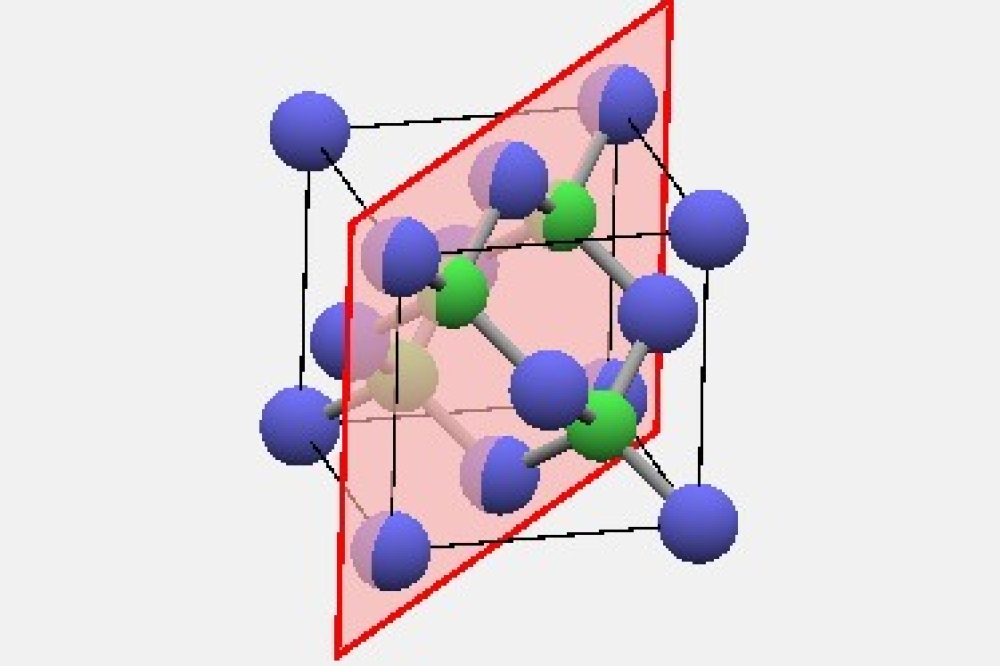
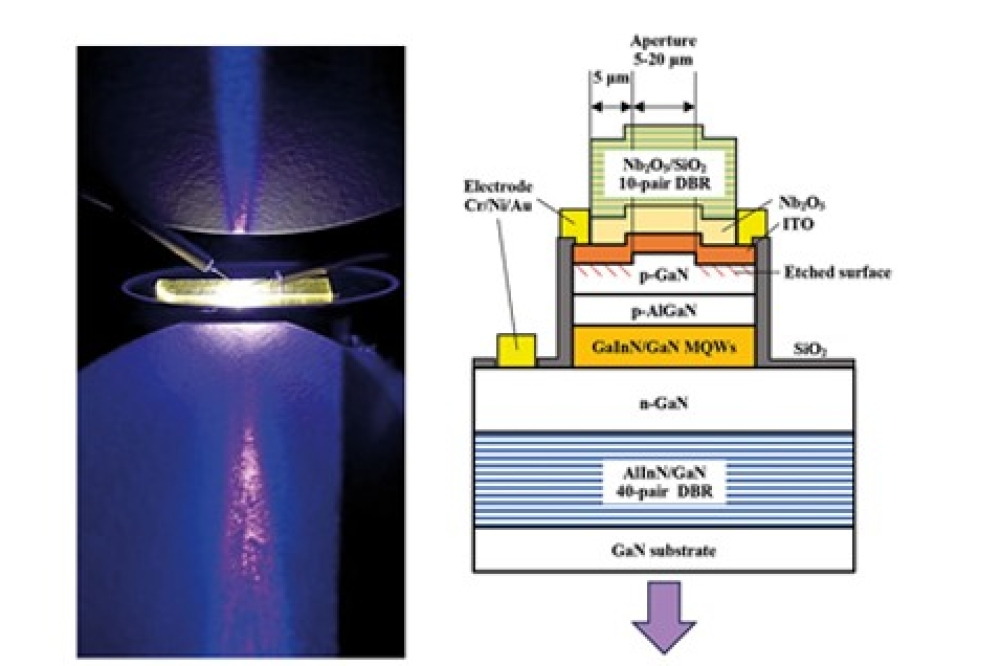
The latest triumph for Takeuchi and co-workers follows many years of work directed at improving their process for producing GaN-based VCSELs. This class of laser features either a pair of dielectric mirrors, or a dielectric top mirror and a bottom mirror formed from alternating layers of AlInN and GaN. The latter simplifies the fabrication process, as there is no need to remove the substrate. However, growth of a high-quality mirror from 40 pairs of AlInN and GaN is far from trivial.
To improve the quality of this mirror, Takeuchi and colleagues initially cleaned the AlInN surfaces with thermal hydrogen processes, before more recently adding an in-situ measurement of the reflectivity spectra, to increase control over the cavity thickness. Prior to the latter refinement, a ± 2 percent deviation in growth rate threatened to deviate the cavity resonance wavelength by ± 8 nm, potentially shifting the resonance wavelength towards the edge of the stop band for the mirror. This concerning state-of-affairs, which could impede device performance, has recently been addressed with the introduction of in-situ monitoring, which ensures a cavity length within 0.5 percent of the target wavelength.
Building on this breakthrough, the team is now calibrating the thickness of the ITO layer and the N2O5 spacer layer, using vertical-cavity test structures.
Part of the reason for taking this particular approach is that the engineering team does not have access to a sputtering system featuring in-situ monitoring, according to Takeuchi: “Another is that the total thickness is just one-tenth of the total thickness of GaN-based layers in the cavity, so that the thickness deviation of ITO/N2O5 is not very critical.”
Investigations featuring 10 mirror pairs of AlInN and GaN determined that when sputtering ITO and N2O5, the control accuracy, in terms of resonance wavelength, is ±3 percent. However, as the team’s VCSEL design employs a 4l-cavity, and the thickness for the two oxide layers is just 0.3l, the actual thickness deviation resulting from this pair of oxide layers is roughly half that for the GaN-based 3.7l cavity.
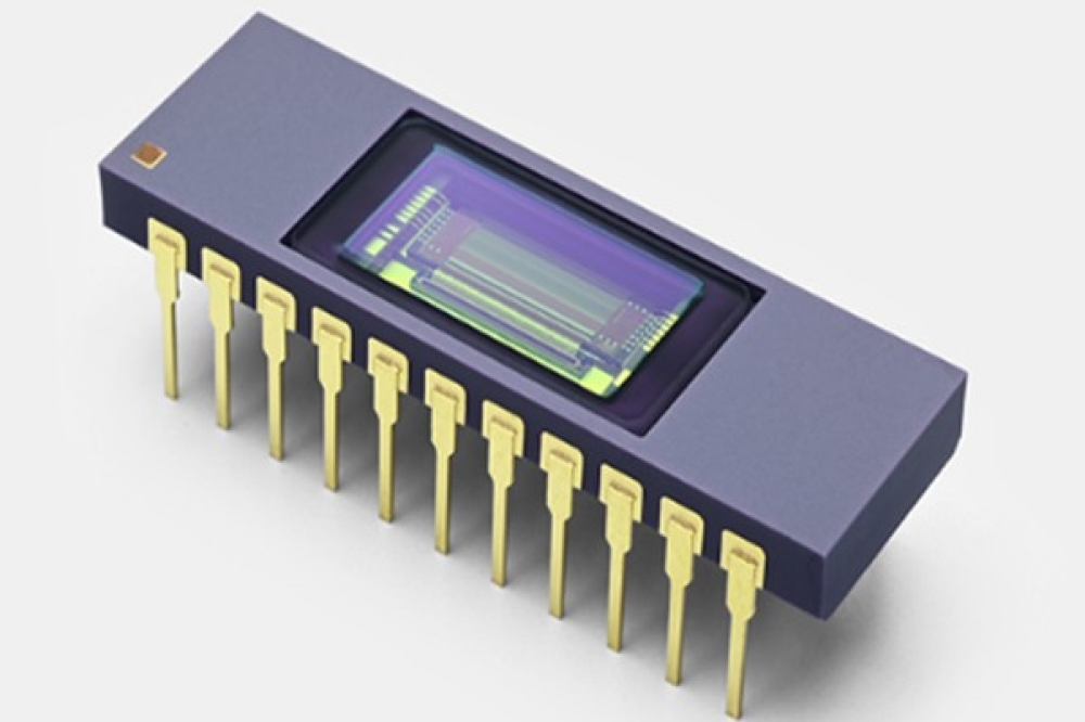
The team incorporated this design of cavity into a portfolio of VCSELs featuring 5 nm-high mesas with diameters of 5 mm, 8 mm, 10 mm, 15 mm and 20 mm. Defined by dry etching with BCl3, the mesas ensure lateral current and optical confinement.
On-wafer measurements by the team revealed lasing at 417.7 nm, just a 0.1 percent deviation from the target of 418 nm. The variant with an 8 μm-diameter aperture produced the most powerful emission, peaking at 13.1 mW, three times higher than the team’s previous best. For wall-plug efficiency, the design with the 5 mm-diameter aperture delivered the most impressive performance, with efficiency peaking at 21.3 percent – realised at 8.44 mA, a drive current that produced an output power of almost 10 mW.
Takeuchi believes that packaging would improve device performance, but not by much. He and his colleagues are now trying to increase the wall-plug efficiency to around 40 percent.
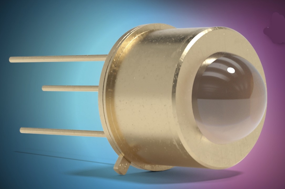
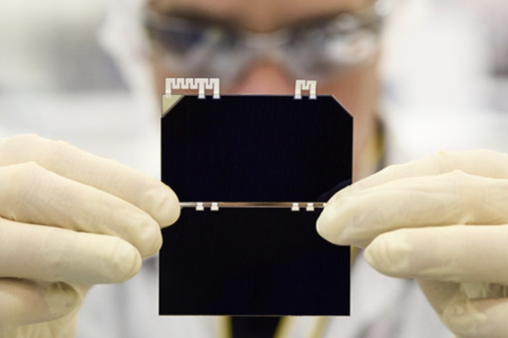
Pictured above: A 5 nm-high mesa ensures lateral current and optical confinement.
Reference
R. Watanabe et al. Appl. Phys. Lett. 124 131107 (2024)