Realising a low contact resistance on N-polar GaN
A team from Nagoya University and Ulvac is claiming to have developed a novel low-temperature process for producing ohmic contacts on N-polar GaN surfaces.
Forming an ohmic contact on these surfaces is far more challenging than it is on Ga-polar surfaces, present in the more mature forms of GaN transistor. However, a process for adding ohmic contacts to N-polar GaN surfaces is needed when producing vertical power devices, as well as N-polar HEMTs, a promising class of device for RF amplification.
To produce ohmic contacts on the more common Ga-polar surface, engineers grow heavily doped epitaxial layers of GaN on the topmost surface, before depositing metals and sintering and annealing them. But that’s far from ideal for N-polar surfaces. During fabrication of vertical GaN-based devices, the substrate is ground and polished to trim thermal and electrical resistance, before attempting to add a low-resistance contact to this layer. For the last step, a temperature below 600 °C is required to prevent processing from degrading device performance. This rules out: using MOCVD on n-type GaN on N-polar surfaces, as that requires temperatures in excess of 1,000 °C, and ion-implantation, which involves activation annealing at temperatures beyond 1,000 °C.
Offering a promising alternative is a sputtering-based approach employed by the team from Japan. According to spokesman Shinji Yamada from Nagoya University, their technique for forming GaN is unique, involving a surface reaction between liquid-phase gallium and nitrogen radicals.
Yamada is not the first to sputter GaN on N-polar surfaces, with success reported on that front last year by Hiroshi Fujioka’s group from the University of Tokyo. Results from that team focused on crystallinity, carrier concentrations, mobilities, surface morphology and photoluminescence.
“On the other hand, our report focused on properties such as contact resistances, considering the contact formation process for GaN devices.”
Yamada and co-workers formed heavily germanium-doped n-type GaN films on an N-polar GaN surface using radical-assisted reactive GaN sputtering. Liquid-phase gallium and a nitrogen radical gun were used as the sputtering sources, and a germanium target provided an n-type dopant.
After reaching the substrate surface, the sputtered gallium and germanium particles, and the nitrogen radicals, undergo chemical reactions to form a GaN film.
To assess the quality of the GaN films produced by this process, the researchers took semi-insulating substrates produced by HVPE and thinned them to 50 mm by grinding and chemical mechanical polishing the N-polar surface. Cleaning with organic solvents and acid solutions followed, prior to the addition of GaN via sputtering, using a range of conditions.
For sputtering, the team varied the germanium-to-gallium sputtering ratio from 0 to 0.15 while maintaining a constant gallium sputtering power, and used substrate temperatures of 500 °C and 600 °C.
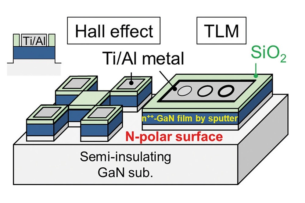
Following GaN growth, the team created structures for electrical measurements (see Figure) that featured a Ti/Al metal stack, deposited by an electron-beam evaporator. Sintering at 475 °C under nitrogen gas for 5 minutes created an ohmic contact.
Transmission electron microscopy revealed that the GaN film sputtered at 600°C is epitaxial, while that deposited at 500°C is only epitaxial in most parts, and riddled with many defects, including stacking faults and inversion domains.
According to Hall-effect measurements on contacts formed at 500 °C, increasing the proportion of germanium to gallium increased the carrier concentration, with a sputtering ratio of 0.15 producing a concentration of 2.6 x 1020 cm-3. The corresponding contact resistance is 9.4 x 10⁻⁵ W cm2, a value indicting a low specific contact resistance. For contacts formed at 600 °C, the researchers only considered a sputtering ratio of 0.11, which led to a carrier concentration of 1.8 x 1020 cm-3 and a contact resistance of 2.0 x 10⁻⁵ W cm2.
Yamada and co-workers are now considering the application of heavily-doped n-type GaN films to a range of GaN devices.
Picture above: To assess contact resistance, structures were produced for Hall effect and transmission line measurements.
Reference
S. Yamada et al. Appl. Phys. Express 17 036501 (2024)