Loading...
News Article

1200V GaN HEMTs in the pipeline

News

Fraunhofer IAF reveals work on GaN-based alternatives to SiC MOSFETs

At the PCIM Europe exhibition in Nuremberg, researchers at the Fraunhofer Institute for Applied Solid State Physics IAF have revealed they are working on GaN-based HEMTs with blocking voltages up to and above 1200V for applications such as two-way charging of EVs. The aim is to replace SiC MOSFETs with a more cost-effective alternative.

Fraunhofer IAF is also pursuing several other approaches: the processing of GaN HEMTs on silicon substrates (GaN-on-Si HEMTs); the use of highly insulating carrier substrates such as sapphire, SiC or also GaN (GaN-on-insulator HEMTs); and the development of vertical GaN technologies.

Lateral GaN-on-Si HEMTs are already commercially available, but are limited to a blocking voltage of 650V due to limited GaN layer thicknesses. By continuously optimising the material and its processing (epitaxy, processing, structuring), researchers at Fraunhofer IAF have been able to demonstrate GaN-on-Si HEMTs with static blocking voltages of over 1200V.

In the second approach, the researchers replace the conductive Si with highly insulating carrier substrates such as sapphire, SiC or GaN, which virtually eliminates the voltage limit. Lateral GaN-on-sapphire HEMTs can be manufactured cost-effectively based on relevant preliminary work for LED applications and can be produced in existing production lines.

Vertical GaN technologies, in which the current flow runs vertically through the material layers, enable even greater performance with higher efficiency and integration capability at the same time. Within the next decade, the researchers at Fraunhofer IAF want to make vertical GaN power ICs suitable for industrial use.

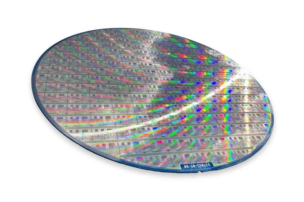
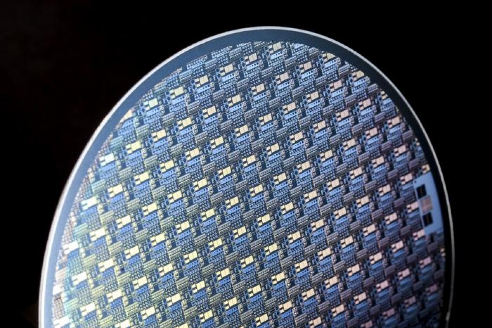
Pictured above: GaN-on-Si wafer comprising vertical components, developed by Fraunhofer IAF

SPONSOR MESSAGE

Secure Your Hydrogen Supply

A study supply of high-purity hydrogen is critical to semiconductor fabrication. Supply chain interruptions are challenging manufacturers, leading to production slowdowns and stoppages. On-site hydrogen generation offers a scalable alternative for new and existing fabs, freeing the operator from dependence on delivered gas.

Plant managers understand the critical role that hydrogen plays in semiconductor fabrication. That important job includes crystal growth, carrier gas, wafer annealing, and in the emerging Extreme UV Lithography (EUV) that will enable new generations of devices. As the vast need for semiconductors grows across all sectors of world economies, so does the need for high-purity hydrogen.

Take control with Nel on-site hydrogen generation.

Read more
Ascent wins order for power beaming Space PV module
Navitas Partners with Great Wall for 400V-DC power
SemiQ supplies SiC MOSFET modules for EV battery cell cyclers
Coherent and Keysight collaborate on 200G/lane multimode VCSEL tech
Lumentum and Marvell exhibit integrated 450G optical interface
Marktech announces new MWIR LEDS
Imec identifies stable range for GaN MISHEMTs in RF PAs
Polar Light completes $3.4m funding round
Lynred launches advanced thermal imaging modules
Altum RF expands Sydney design centre
Sivers announces partnership with O-Net
Ayar Labs unveils first UCIe optical chiplet
Aixtron delivers InP tool to Nokia
WHU-USTC team demo novel temperature monitoring of GaN device
Phlux lands £9m to take InGaAs sensors to next level
4-inch gallium oxide facility established in Swansea
Mazda and Rohm collaborate on automotive GaN
University of South Carolina chooses MOCVD tool from TNSC
Wolfspeed appoints new CEO amidst funding crisis
SiC slowdown is only short term, says Yole
Pragmatic launches flexible IGZO-based NFC chip
Poet ships latest optical engine samples
EU project to develop 1200V DC powertrain
£250m to turbocharge Welsh compound semi cluster
Scientists harness phonon-polariton electroluminescence
TU Graz team reveals the secrets of heat conduction
Aixtron to partner in ‘GraFunkL‘ UVC project
EU collaboration steps up heterogeneous design
Diodes Inc announces InSb sensors
Far-UVC module targets close-quarters disinfection
Sivers and WIN collaborate on DFB laser production
Boosting the blocking voltage of birectional HEMTs
×
Search the news archive

To close this popup you can press escape or click the close icon.
Logo
x
Logo
×
Register - Step 1

You may choose to subscribe to the Compound Semiconductor Magazine, the Compound Semiconductor Newsletter, or both. You may also request additional information if required, before submitting your application.


Please subscribe me to:


You chose the industry type of "Other"

Please enter the industry that you work in:
 
x
Adblocker Detected
Please consider unblocking adverts on this website