2D-Mg doping improves p-type GaN conductivity
Researchers at Nagoya University have discovered that annealing bare metallic Mg film on GaN forms a unique structure where single-atomic Mg layers periodically insert into GaN. This new structure, termed 2D-Mg intercalated GaN superlattice (MiGs), represents a novel doping and straining mechanism for semiconductor and thin-film materials. The findings were published in Nature.
To improve p-type GaN conductivity, Jia Wang, Hiroshi Amano, and their colleagues deposited metallic Mg thin films on GaN and and heated it up at a high temperature — a conventional process known as rapid thermal annealing. Using state-of-the-art electron microscope imaging, they observed the spontaneous formation of a superlattice featuring alternating layers of GaN and Mg. This is especially unusual since GaN and Mg are two types of materials with significant differences in their physical properties.

Figure: microscopic images and schematic of the 2D-Mg intercalated GaN Superlattice (MiGs)
By examining the lattice constants of GaN and Mg, the researchers found that although GaN and Mg are disimilar materials, both have the same crystal structure with negligible differences in their lattice constants. This 'perfect match' in lattice structure between GaN and Mg significantly reduces the energy required for the spontaneous formation of the superlattice, playing a crucial role in its formation. Similarly, for the same reason (perfect lattice matching between GaN and Mg), it can explain the tendency of Mg to form coherent segregation in GaN, thus solving the mystery of the low solubility and segregation tendency of Mg in the GaN lattice.
The 2D-Mg atomic layer can reverse GaN polarity, as confirmed by iDPC-STEM images. GaN transitions from N-polarity to Ga-polarity between 2D-Mg layers. These polarity changes induce space charges, similar to those in compositionally degraded AlGaN. Thus, 2D-Mg layers create periodic polarity gradients in GaN, generating negative space charges and potential holes. This novel '2D-Mg' doping phenomenon differs from traditional substitutional Mg impurity doping (0D-Mg doping).
Microstructural observations also revealed a unique interstitial-type intercalation phenomenon. The interstitial intercalation induces high elastic strain in the matrix atomic layers. STEM imaging confirmed GaN's uniaxial compressive strain exceeds -10 percent. Given GaN's high elastic modulus (>200 GPa), the corresponding elastic stress value over 20 GPa is a record for experimentally observed elastic stress in materials.
Elastic strain in semiconductor materials can alter band structures. GaN's valence band structure consists of heavy hole (HO), light hole (LO), and split-off (SO) bands. Theoretical predictions suggest that when GaN's compressive strain along the c-axis surpasses a certain value, the SO band will dominate the valence band, rising above the HO and LO bands. Since the SO band holes' effective mass along the c-axis is about 1/10th that of heavy holes, this implies that sufficient uniaxial compressive strain can significantly increase hole mobility and improve p-type GaN conductivity along the compression direction.
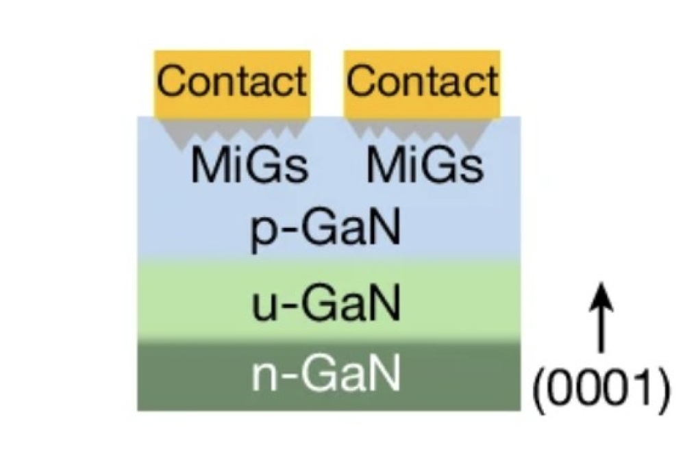
In electronic devices, incorporating MiGs structures on low-doped n-type GaN surfaces can raise the Schottky barrier height, proving the 2D-Mg-induced negative space charges. Furthermore, incorporating MiGs structures on p-type GaN surfaces can also achieve excellent ohmic contact, addressing a bottleneck issue for p-type GaN. The simple and cost-effective synthesis method offers considerable industrial value.
Future research will focus on the precise artificial synthesis of uniformly distributed MiGs structures from initial naturally formed observations.
Reference
Wang, J., Cai, W., Lu, W. et al. Observation of 2D-magnesium-intercalated gallium nitride superlattices. Nature (2024)