EVG and Fraunhofer IZM-ASSID expand partnership
Wafer bonding and lithography equipment company EVG and research organisation Fraunhofer IZM-ASSID (All Silicon System Integration Dresden) have entered into a partnership to develop and optimise alternative bonding and debonding technologies for advanced CMOS and heterogeneous integration applications, including quantum computing.
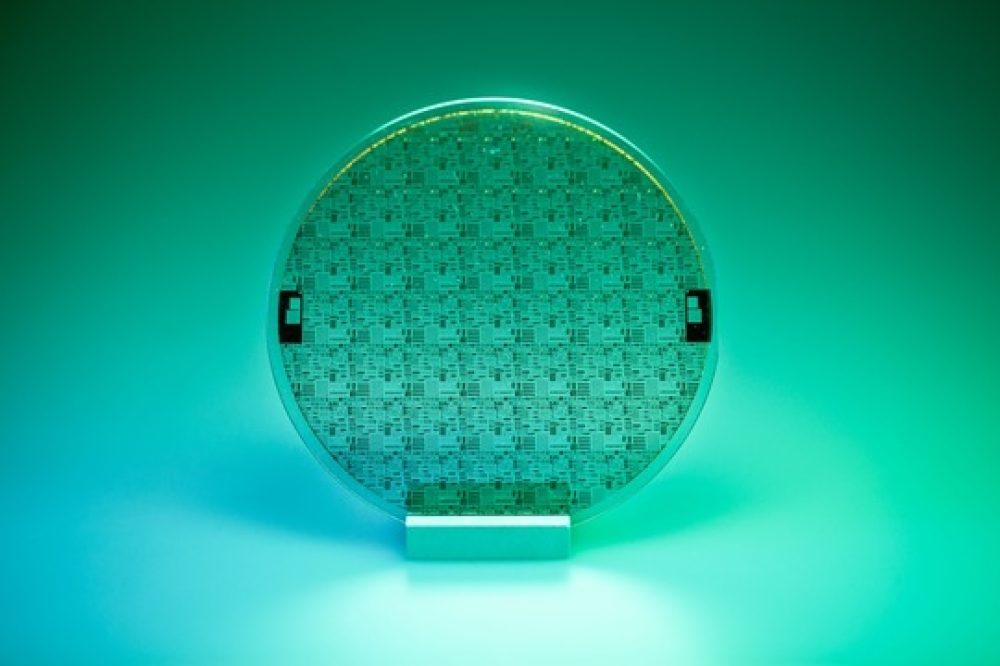
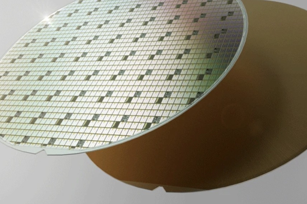
EVG’s wafer bonding, lithography and metrology solutions enable the development and high-volume manufacturing of technology innovations in advanced packaging — including backside illuminated CMOS image sensors and other 3D-IC stacked devices—as well as in MEMS and compound semiconductors.
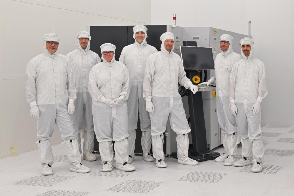
Kicking off this expanded collaboration, Fraunhofer IZM-ASSID has purchased and installed an EVG 850 DB fully automated UV laser debonding and cleaning system at Fraunhofer’s newly established Center for Advanced CMOS and Heterointegration Saxony, located in Dresden, Germany.
CEASAX combines core competencies from Fraunhofer IZM-ASSID and the Fraunhofer Institute for Photonic Microsystems (IPMS) to further research into 300mm, 3D heterogeneous wafer-level system integration and front-end semiconductor integration processes for high-performance neuromorphic computing, cryo- and quantum technology.
The EVG850 DB is the first system to be installed at CEASAX, and will help enable Fraunhofer IZM-ASSID to close critical process gaps and offer technology modules for the manufacturing of quantum systems and their wafer-scale hardware environment based on a 300-mm cleanroom environment. The system’s installation also marks the start of Fraunhofer’s Bond-Hub, which will additionally comprise a multitude of leading-edge temporary as well as permanent wafer-to-wafer and die-to-wafer bonding systems.
“Fraunhofer and EV Group have enjoyed a long and successful collaboration in developing new processes that have helped enable critical, emerging micro-electronics applications – including multi-device integration of analog and digital devices such as ASICs, RF devices, sensors and transceivers into an optimised system-in-package or functional smart microelectronic systems,” stated Manuela Junghähnel, site manager, Fraunhofer IZM-ASSID. “
We are excited to be expanding and reinforcing this partnership through the purchase of the EVG850 DB laser debonding and cleaning system, which will be the first of several key product installations at CEASAX, our new advanced semiconductor research center. Through this expanded relationship, Fraunhofer will receive state-of-the-art technology in-house and have a strong partner in EV Group for developing new technologies for 3D device integration, which in turn will offer our customers a more complete process chain for 3D/heterogeneous integration from a single source.”