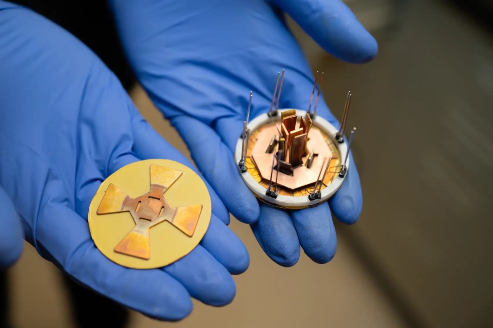
Scientists test GaN chips inside nuclear reactor
Researchers at the US Department of Energy’s Oak Ridge National Laboratory are working to make the sensors used inside nuclear reactors more accurate by pairing them with GaN-based electronics that can withstand the intense radiation inside a reactor.
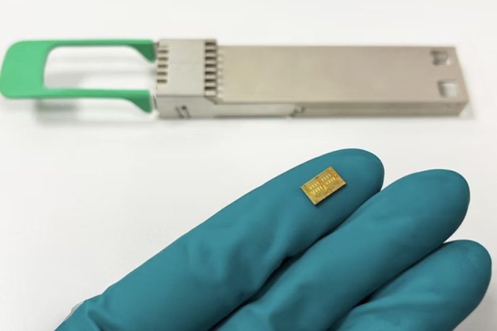
A transistor made with the material has recently maintained operations near the core of a nuclear reactor operated by research partner The Ohio State University.
GaN has previously been tested against the ionizing radiation encountered when rockets hurtle through space, but has not faced the even more intense radiation of neutron bombardment. “We are showing it is great for this neutron environment,” said lead researcher Kyle Reed, a member of the Sensors and Electronics group at ORNL.
The researchers think it could offer a big boost for equipment monitoring in nuclear facilities. The information gathered by sensors provides early warnings about wear and tear on equipment, allowing timely maintenance to avoid broader equipment failures that cause reactor downtime. Currently, this sensing data is processed from a distance, through yards of cable connected to electronics with silicon-based transistors.
“Our work makes measuring the conditions inside an operating nuclear reactor more robust and accurate,” Reed said. “When you have lengthy cables, you end up with a lot of noise, which can interfere with the accuracy of the sensor information. By placing electronics closer to a sensor, you increase its accuracy and precision.” To meet that goal, scientists need to develop electronics that can better tolerate radiation.
Researchers irradiated GaN transistors for three days at temperatures up to 125 degrees Celsius close to the core of The Ohio State University Research Reactor. “We fully expected to kill the transistors on the third day, and they survived,” Reed said. The team pushed the transistors all the way to the reactor’s safety threshold: Seven hours at 90 percent power.
The GaN transistors were able to handle at least 100 times higher accumulated dose of radiation than a standard silicon device, said researcher Dianne Ezell, leader of ORNL’s Nuclear and Extreme Environment Measurements group and a member of the transistor research team.
She said the transistor material needs to be capable of surviving at least five years, the normal maintenance window, in the pool of a nuclear reactor. After the research team exposed the GaN device to days of much higher radiation levels within the core itself, they concluded that the transistors would exceed that requirement.
This is an important technical advance as attention turns from the large-scale existing fleet of nuclear energy plants to microreactors that could generate from tens to hundreds of megawatts of power. Although these novel reactor designs are still in the development and licensing stage, their potential portability could allow them to be deployed on the back of a truck to a military or disaster zone.
Advanced reactors are being designed to operate at higher temperatures using different forms of fuel. Because microreactors will be so compact, all the operating components, including the sensors, will have to be able to function in the radiation field, Ezell said. GaN transistors could be the key.
Ohio State researchers built devices of different designs and sizes to meet specifications set by ORNL, and then the team compared their responses to radiation, finding that larger devices seemed less susceptible to radiation damage. Ohio State is now developing computer models to project how various circuit designs will perform under different temperatures and radiation levels.
Reed said the radiation testing at Ohio State showed that heat seemed to be more harmful to the GaN than radiation. So, the research team wants to measure how GaN reacts to heat alone. “Since the ultimate goal is to design circuits with these materials, once we understand the temperature and radiation effects, we can compensate for them in the circuit design,” Reed said.
In the long run, researchers would like to demonstrate that GaN circuits could be used to transmit data from sensors wirelessly. The material is already used for devices that support radio frequency applications, like cell phones, and for power electronics.