Nanowires eye augmented-reality displays
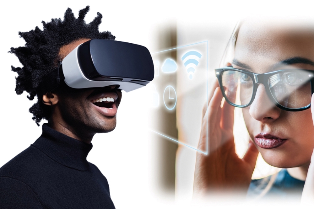
The mass market seeks augmented-reality displays small enough to embed in a pair of sleek, lightweight eyeglass frames.
BY SETH COE-SULLIVAN FROM NS NANOTECH
When Apple shipped its first Vision Pro headsets this February, it joined a battle with Meta and other manufacturers for a share of the emerging global market for virtual reality (VR), augmented reality (AR), and mixed reality (MR) applications. But the Vision Pro’s large form factor and its hefty price tag raised as many questions as Apple answered in its presentation on the future of a new age of ‘spatial computing’.
Initial reviews noted that, like the popular Meta Quest headsets, the Vision Pro is large, bulky, and generally too heavy for all-day use. And while it offers spectacular immersive video and audio experiences, this comes at a hefty price. Retailing at $3,499, the Vision Pro is four-to-five times as expensive as its competitors.
Unfortunately, all of these rivals, which are capable of demonstrating the exciting possibilities of AR, MR, and VR applications, are held back by several issues. Today they are not small enough, are limited in efficiency, not easy to manufacture, and lack the affordability that would see many consumers make them a constant companion. The mass market wants to go beyond those headsets that resemble oversized ski goggles for immersive VR and MR applications, and move to AR displays that are small enough to embed in a pair of sleek, lightweight eyeglass frames that one can comfortably wear all day.
Delivering AR displays that are this small and efficient is far from easy. It demands advances in a range of technologies, starting first and foremost with a reduction in the size of the display. The bulk required for smart AR features to be added to a normal pair of glasses is determined largely by the display size, which governs the size of the waveguides, battery, mechanical parts, and other optical components necessary to deliver satisfying AR images. Today’s displays that are suitable for AR are still far too large to integrate with normal-sized eyeglasses. And because weight is largely determined by the size of the battery required, displays with greater efficiency are needed to ensure smaller power sources. Therefore, today’s displays that are based on microOLED and microLED emitters, small as they are, will need to be even smaller and far more efficient.
‘Bottom-up’ fabrication
One promising approach to realising these much-needed size and efficiency breakthroughs is to turn to nanowire-based LEDs. It is possible to integrate these submicron-scale emitters into displays that are small enough for a standard pair of eyeglasses (see Figure 1).

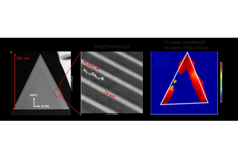
Figure 1. A single submicron-scale nanowire can be a complete LED (left). However, in most cases tens to hundreds of nanowires will make up a single sub-pixel of a full colour display (left-centre). LEDs can then be integrated on an red-green-blue display (right-centre) that’s small enough to fit unobtrusively into a standard pair of eyeglass frames (right).
Many of the early developers of this revolutionary technology are growing GaN nanowires on silicon or sapphire substrates with a core-shell architecture featuring a p-GaN shell and an n-GaN core. It is hard to overstate the potential benefits of these efficient nanowire LEDs. Individual microscopic nanowire LEDs, bundled and working in concert on a standard semiconductor substrate, have the potential to combine an extremely high efficiency at higher brightness with much lower costs and longer lifetimes than today’s LEDs and microLEDs. Allied to this, there is the use of simpler fabrication processes, offering the potential to scale-up mass production while minimising defects and delivering higher yields.
However, current nanowire LEDs and microOLEDs have yet to fulfil their promise. They are failing to deliver the brightness and efficiency that’s required to meet the demanding requirements of future AR displays. What’s more, they do not yet emit red or green light, and they require either filters or a layer of quantum dots to convert the blue emission to the red and green to create colour displays – and this adds to device manufacturing complexity and cost. On top of all these concerns, when the quantum dot down-conversion approach is scaled to a 1 µm pixel size, an efficiency loss results, undermining the advantages of the microLED.

Figure 2. Multi-colour nanowire LEDs as small as 100 nm are grown on submicron-scale pixels (left); MBE ensures control of the growth and placement of atoms into single nanocrystals on standard substrate materials (right).
But let’s not throw the baby out with the bathwater. It is possible to retain nanowire LEDs, but make them even smaller, by growing nanowires from the bottom up, rather than building them out from the core to the shell. This is the approach we are trailblazing at NS Nanotech that will meet the requirements of AR displays.
Our approach, which draws on the work of Zetian Mi’s group at the University of Michigan, has led to the first submicron-scale nanowire LEDs (see Figure 2). It is a technology that enables each nanowire to operate as a complete LED, all the way down to 100 nm in diameter, that can be tuned to emit any desired colour.
Taking a bottom-up approach represents a marked and welcome departure from traditional LED fabrication. There are downsides associated with planar LEDs, which have to battle against the challenges of materials physics, which begin with full-size LEDs and continue when trimming these emitters down in size to make them mini and eventually micro. Core-shell fabrication circumvents scaling issues through the growth of individual nanowires. However, with this architecture recombination zones are formed on sidewalls, a process that limits efficiency and colour tunability.

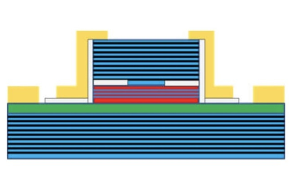
Figure 3. Nanowires grow from the bottom up without an additional process for a separate shell. While growing atomically precise quantum wells, higher bandgap material flows to the outside of each column, protecting quantum wells from the surface states and ultimately resulting in high internal quantum efficiencies (IQEs).
The approach that’s been developed by Mi avoids all these pitfalls. Device production starts from the bottom up, with a process that creates discrete, independent LED nanocrystals that are grown directly up from the substrate and utilise a layered structure that is very similar to conventional planar LEDs. This approach has enabled laboratory demonstrations of the first efficient submicron-scale red and green nanoLEDs – they deliver world-record internal and external quantum efficiencies.
To transfer these innovations from the lab to the fab, Mi co-founded NS Nanotech, which has exclusive licenses to patents from his work at University of Michigan and McGill University. Our spin-off is currently conducting further research on his novel approach to nanowire growth, while working on fabrication techniques that will provide the reproducibility and scalability required for mass manufacture of nanoscale LEDs.
Four key breakthroughs
Our nanowire growth technique is underpinned by four technical breakthroughs in materials science. These breakthroughs leverage three pre-existing foundational technologies: MBE, which enables unparalleled control of the growth and the placement of atoms into single nanocrystals on standard substrate materials; nitride semiconductor technology, which provides the most stable light emitters in existence; and the nanostructures themselves.
The four materials science technology breakthroughs that come from Mi’s group and build on those three pre-existing foundational technologies are catalyst-free nanocolumn growth, a disc-in-nanocolumn architecture, the use of a photonic bandgap, and monolithic integration on any substrate. We shall now discuss each in turn.
When growing nano-columns, there is an advantage to avoiding catalysts, which threaten to lead to purity problems and ultimately diminish electroluminescence efficiency. However, there are those that will tolerate this concern, pointing out that when nanowires are anchored to a surface, as opposed to being grown colloidally, it is easier to realise electroluminescence.

Figure 4. A periodic lattice, which has a pitch that’s just a fraction of the wavelength of light that’s being emitted, creates a photonic bandgap that overlays the semiconductor bandgap. The upshot is laser-quality spectral purity and directionality.
Fortunately, though, it’s possible to enjoy the best of both worlds, thanks to Mi’s development of a new method that is capable of growing high-purity nitride semiconductor material from almost any surface, while realising full doping control that allows for facile creation of LEDs. This ground-breaking technique enables the growth of GaN nanowires with regions of p-type and n-type doping, defined during epitaxy, along with alloying. Adding indium leads to visible emission, while the incorporation of aluminium ensures ultraviolet electroluminescence. Additional merits of catalyst-free nanocolumn growth are selective-area growth or selective-area epitaxy, realised with positional placement, accuracy, flexibility, and control over the packing density.
The disc-in-a-nanocolumn architectures, which are sometimes referred to as dot-in-a-wire nanostructures, offer a number of benefits. They include the reduction or elimination of crystallinity defects, surface trap states, and non-radiative emission pathways – all of which kill efficiency.
However, while the disc-in-a-nanocolumn architecture works on paper, it is complex to implement. From a perspective of chemistry process flow, there’s a lot of sense to growing core-shell nanocrystals in solution, from the inside out. But growing the shell – that’s the sheaths on the outside of the column – is extremely difficult.

Figure 5. A lithographically defined mask enables growth of nanowires of any shape, size, and colour, in any location on the substrate (left). Adjusting the diameter of the nanowires tunes the emission wavelength and the resulting colour of light (right). Source: Photonics Research, 2022.
One way to avoid this issue, developed by Mi’s group, is to utilise the natural differences in atomic migration along the crystal surfaces. Adopting this approach enables the creation of aluminium-rich regions and indium-poor regions in the crystal, while growing the nanowire from the bottom up without an additional process for a separate shell. During the growth of atomically precise quantum wells, higher bandgap material flows to the outside of each column, protecting the wells from surface states.
The result is material with incredibly high internal quantum efficiencies, especially in the green and red. Efficient emission at these longer wavelengths stems from the use of MBE, which locks these high-indium-content wells away from thermal equilibrium, while the disc-in-a-column architecture lets them emit at high efficiency, unlike conventional nanowire or planar approaches. These innovations eliminate process steps while avoiding some of the problems presented by core-shell architectures (see Figure 3).
The photonic bandgap associated with our nanoscale LED ensures a more stable emission profile over its planar cousins. The instability stems from emission that is only governed by the semiconductor bandgap, a condition that leads to colour drift problems when the doping level isn’t perfectly controlled, or when the device heats up.
Our microLEDs avoid this weakness. Our columns are smaller than the wavelength of light, and we place them with sub-nanometre accuracy, using 2D lithography. We design these columns into a periodic lattice with a pitch that’s just a fraction of the wavelength of the light being produced, to create a photonic bandgap that overlays the semiconductor bandgap. Running current through the nanocolumns creates electron-hole pairs across the semiconductor bandgap that are ready for spontaneous emission and, when resonant with the photonic cavity, emit far faster and at exactly the same frequency. Photons leap out of this cavity in exactly the same cone, creating very directional light without any waveguiding. The result is laser-quality directionality from a speckle-free diode (see Figure 4).

Figure 6. Nanowires grown in the lab create submicron-scale LEDs with external quantum efficiencies of 8 percent in the red and 25 percent in the green. These performance levels equal or exceed standard-size LEDs that are orders of magnitude larger.
Another strength of our approach is that it enables monolithic integration on any substrate. The substrate is not an issue, as nanocolumns can grow defect-free on almost anything. Sapphire is convenient, silicon easier, and it is even possible to grow our nanowires on a metal surface or foil. On all of these foundations and more, we can place the nanocolumns arbitrarily while controlling their shape and size.
What’s more, through understanding how the atoms migrate as they deposit, we can use their diameter to control their colour. We have established that wider columns incorporate less indium into their discs than narrow ones, proving another opportunity to control the emission colour in a predictable manner. Through controlled variation in the diameter of the columns, we can create red, green and blue sub-pixels on the same substrate, at the same time, in a single growth step. And by adding yellow pixels, we can grow LEDs in four colours in a single step. We have even shown that it is possible to turn-on single-wire devices of different colours, positioned adjacent to one another and located within a single square micron of area.
Contrary to typical nanowires that are randomly positioned, thanks to selective area epitaxy, we enjoy precise control of nanowire spacing, location, and diameter through lithographic patterning and growth (see Figure 5). Many advantages result from this, including an opportunity to tune the emission wavelength and the resulting colour of light by adjusting the nanowire’s diameter. We gain this degree of control by adding a single lithographically defined mask step, inserted after template growth but prior to the growth of the nanowires. It is the selectivity of the mask that allows us to make nanowires where we want them, in the shape, size, and colour of our choosing. This is key to our delivery of the first true sub-micron-scale ‘nano LEDs’ with the potential to deliver a performance that’s superior to today’s LEDs, realised at much lower costs and in a small enough form factor to meet the requirements of next-generation AR displays.

Figure 7. A single nanowire-based red LED is ten times more efficient and a million times smaller than standard red LEDs with comparable efficiency.
Record reds and greens
Due to the nanostructure nature of our nanowire LEDs, high material quality is a given, even for indium-rich layers. And MBE enables growth at low enough temperatures to prevent indium from evaporating from the InGaN surface during growth. Taken together, these advances in materials technology are delivering the performance levels required to make nanowire-based displays commercially attractive.
Strong evidence of this capability is provided by progressive world records for the performance of devices created in the lab. We have measured green nanoLEDs with a 25 percent external quantum efficiency, a performance level on a par with today’s planar LEDs that are orders of magnitude larger. For red nanowire LEDs, external quantum efficiency is 8 percent, another world record for sub-micron scale LEDs. This level of performance is well ahead of the pack, with efficiency about ten times higher than the next-best red LED of the same size – and around a million times smaller than the next-best red InGaN LED at this efficiency (see Figures 6 and 7).

Figure 8. Separate growths of nanowires on non-consecutive days yield indistinguishable results – evidence that the nanowire LED fabrication process is repeatable, and that MBE is stable enough to perform identical processes consistently.
From lab to fab
Manufacturing nanowire-based LEDs at scale for mass markets requires scalable fabrication processes that ensure uniformity and reproducibility of nanowire growth at the wafer scale. To this end, we are determining process windows for MBE that provide repeatable, uniform results. We are encouraged by our initial efforts, demonstrating the repeatability of nanowire growth (see Figure 8).
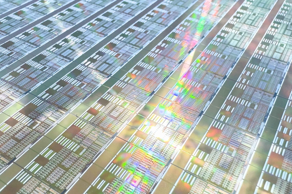
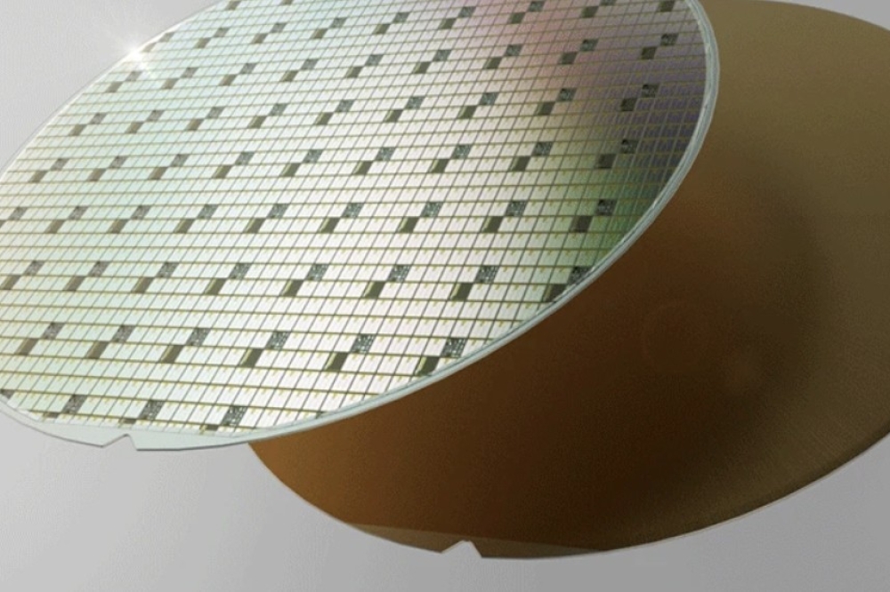
Up until now, we have employed electron-beam lithography for the fabrication of all our laboratory-grown nanowire LEDs. However, this technique isn’t easily scalable for mass production, so we are looking to introduce standard semiconductor processes. They include optical lithography, which is available and pervasive, but until our recent work has never been used to make a nanowire of this type. We have broken new ground by utilising a standard deep-UV optical lithography process on a 100 mm wafer to create a selective-area epitaxy mask. This approach has produced the first ever uniform growth of submicron-scale GaN nanowires on an optically patterned substrate (see Figure 9).

Figure 9. Standard deep-UV optical lithography on a 100 mm wafer resulted in uniform growth of submicron-scale GaN nanowires.
Spurred on by our progress that has enabled us to meet the size and efficiency requirements of microLED displays, we expect nanowire LEDs to enable massive new markets for many, many years, including AR headsets, but also encompassing many other products. By developing the right hardware, including displays and optics, it will be possible to achieve the holy grail of a compelling AR device that can be worn all day – a product that will change how we all interact with computing, and enable a world where we once again turn our heads back up, rather than huddling over our phones.