Ga₂O₃: Improving the gate dielectric
To unlock their full potential, b-Ga2O3 Schottky barrier diodes and various forms of FET demand a high-quality dielectric.
Claiming to meet this need is a team of engineers from the US. These researchers have developed a process for forming HfSiOx, an oxide that is said to combine a high dielectric constant with a large band offset, negligible gate leakage, a low density of interface and bulk traps, and a large breakdown field.
Crucially, the breakdown field for HfSiOx is as high as 8.7 MV/cm, significantly beyond the theoretical breakdown field for b-Ga2O3, of 8 MV/cm. By ensuring that the dielectric has a higher breakdown field than the device, the latter can realise its full potential.
The process for producing a high-quality HfSiOx dielectric on b-Ga2O3 has been developed by a partnership between researchers at the University of Michigan, Union College, and the University of California, Los Angeles. This collaboration has built on its previous work, involving the development of an MOCVD process for producing an AlSiO dielectric on b-Ga2O3. That earlier work produced a dielectric with a breakdown field of around 7.8 MV cm-1.
The increase in breakdown that has resulted from switching to HfSiOx involves a different deposition process. For the latest work, the dielectric is added by atomic layer deposition, prior to an annealing step that ensures significant improvements in important characteristics.
Interest in HfSiOx dates back many years, with previous studies considering its use as a dielectric for devices based on silicon and GaN. Prior work has also shown that by adjusting its composition, the dielectric constant for HfSiOx can range from 3.9 to 27, and the conduction band discontinuity between HfSiOxand b-Ga2O3 can be as high as 2.38 eV.
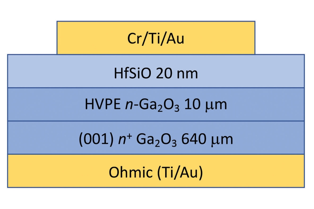
The engineers from the US used metal-oxide-semiconductor capacitors to investigate the performance of the HfSiOx dielectric on b-Ga2O3. They began with epiwafers featuring a 10 mm-thick layer of b-Ga2O3 grown on a heavily n-doped b-Ga2O3 substrate, and turned to atomic layer deposition to add a film of HfSiOx, using a ratio of HfO2 to SiO2 of roughly 1:1. To realise this ratio, two cycles of HfO2 with a deposition rate of 1 Å/cycle were alternated with three cycles of SiO2, with a deposition rate of 1 Å/cycle.
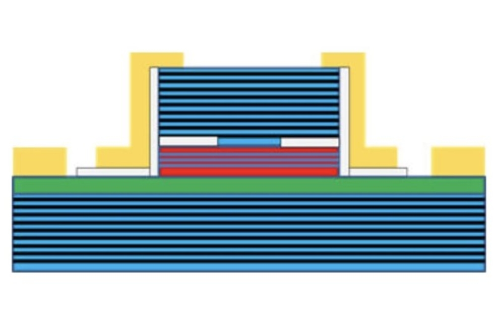
To assess the impact of annealing, the team produced three types of capacitors with 20 nm-thick dielectrics (see figure above). One class avoided any form of heat treatment, while the other two were annealed in nitrogen gas at temperatures of 400 °C and 900 °C.
Breakdown measurements determined that for the unannealed capacitors, low-leakage operation occurs at up to around 3 MV cm-1. Meanwhile, for those annealed at 400 °C and 900 °C, leakage is not seen until 6.2 MV cm-1 and 4.5 MV cm-1, and breakdown fields are as high as 8.4 MV cm-1 and 8.7 MV cm-1, respectively.
Capacitance-voltage measurements, using a deep-UV lamp emitting at 254 nm to provide sufficient hole generation, offered an insight into the level of traps within the dielectric.
Profiles of the unannealed capacitors showed that they fail to reach the accumulation region at low electric fields. The team attributes this observation to an exceptionally high electron-trap-density, both in bulk HfSiOx and at its interface with b-Ga2O3.
Capacitance-voltage measurements determined the total trap densities for both annealed samples. The team reported average values of 2.72 x 1012 cm-2 eV-1 and 1.06 x 1012 cm-2 eV-1 for samples annealed at 400 °C and 900 °C, respectively, indicating that a higher temperature trims the trap density. This led the team to speculate that annealing at 900 °C in an ambient environment reduces oxygen vacancies in HfSiOx and reduces the density of bulk and interface traps.
The engineers have scrutinised their dielectrics with cross-sectional scanning transmission electron microscopy. This technique uncovered partial ordering in the deposited HfSiOx, with annealing at 900 °C creating a fully amorphous dielectric that is behind the reduced leakage current and increased breakdown voltage.
Reference
X. Zhai. et al. Appl. Phys. Lett 124 132103 (2024)