The transistor of the future
Improvements in substrate quality and size, alongside a market primed for accepting new semiconductors, gives the diamond transistor a great chance of commercial success.
BY GAUTHIER CHICOT AND IVAN LLAURADO FROM DIAMFAB
For decades, the diamond transistor has held much promise. However, its performance is yet to fulfil expectations. So why are there grounds for optimism?
That’s a tricky question. One might simply respond with the slightly flippant rebuff: ‘Well, why not?’. But you probably have a healthy degree of scepticism, and demand a more nuanced explanation – and I’m delighted to provide just that, by sharing the vision we have at Diamfab for this technology.
Before we dive into that, let’s begin by recapping the development of diamond for technological applications. The story begins in 1954, when humanity manufactured diamond for the first time, using high-temperature high-pressure techniques. Building on this milestone, the 1980s witnessed the first growth of diamond by CVD, followed by the exploration of doping processes in the 1990s. Since then, those involved in developing synthetic diamond have expanded their knowledge of this material, in terms of characterisation, manufacturing and processing.
As we learn more about the properties of diamond as a semiconductor, the bigger its promise appears – but for some, the bigger the frustration too, as we might have expected a faster development process due to its enormous potential.
The power of diamond
As a material for power electronics, what is the promise of diamond? Well, it has an ultra-wide band gap, an exceptional carrier mobility, a breakdown voltage estimated at a tantalizing 10 MV/cm, and the best-known thermal conductivity. Thanks to these phenomenal attributes, diamond has been called the ultimate power semiconductor. Devices made from this form of carbon have the potential to boost the voltage of components while increasing their efficiency, trimming losses and cutting costs.
To illustrate the gulf in the performance of different materials, think about a basketball and its court. The ball’s surface area represents a diamond component with a given resistance for a 1000 V breaking voltage capacity. And the court? Well, its surface area represents these values for silicon. So, as you can see, there’s a staggering difference in the performance ratio of these two materials in the key figure of merit for power semiconductors.
At the system level, diamond promises to improve all the key characteristics that enable increased power efficiency. Gains come from: simplified thermal management; a better trade-off between increases in the component and system competitiveness/energy efficiency, and a trimming of volume and weight; and a reduction in CO2 emissions, compared with the manufacture of SiC substrates.
These are compelling advantages, giving good reason to be optimistic. And this positive outlook should not diminish when one considers the two biggest factors determining commercial success – the level of technological maturity, and the market situation.
When it comes to technology, three historical roadblocks have to be solved before diamond will become a commercial reality. These barriers are an increase in the size of a diamond wafer, improvements to its quality, and a better approach to doping.
The good news is that all these challenges are being addressed by the diamond industry. At Diamfab, we are making major contributions to this effort, with our development focusing on improving material quality through a reduction in the density of imperfections, and mastering doping.
It’s far from easy to grow large diamond crystals, the starting point for substrate production. For other semiconductor technologies, investment in the research and development of crystal growth has come from defence applications. While that’s also a source of funding for developing diamond, it’s not the only one – it’s also possible to leverage knowledge from other industries, such as jewellery. Drawing on all of this has ensured rapid material progress. Single-crystal wafers with a 100 mm diameter have already been demonstrated, a great advance considering that just a few years ago only 2 mm or 3 mm wafers were commercially available.
The doping of diamond is a considerable challenge. Unfortunately, diffusion and implantation are neither suitable nor recommended. Attempts to dope diamond by diffusion are thwarted by a carbon lattice so dense that potential dopants, such as boron, nitrogen and phosphorus, cannot penetrate into this material. Meanwhile, implantation is hampered by high levels of inefficiency, causing irreparable damage to the crystalline lattice.
Due to these formidable issues, doping must be undertaken in situ, during the growth of diamond. It’s a process we’ve mastered at Diamfab, realising levels of doping that span from the non-intentionally doped, all the way through intermediate values to metal-like levels. We are also making good progress at improving crystal quality, and we expect to announce exciting news soon.
In a nutshell, from both a material and component manufacturing perspective, the primary technological hurdles are either overcome or there is a clear view on how to solve them. And where further progress is required, a great deal can be garnered by studying developments associated with compound semiconductor materials and devices.
In terms of market acceptance, we are living in a world that’s in the midst of revolution, where major megatrends have a common factor: a quest for electrification, sustainability, and efficiency. This is driving demand for efficient power electronics. That’s a stark contrast to the early years of this millennium, when trains, motor drives and UPS accounted for essentially all power electronics – and none of these sectors drove the economy.
The recent trend is highlighted in a BloombergNEF 2023 report, which claims global investment in the energy transition hit a record $1.8 trillion in 2023, up 17 percent on the previous year. With vast sums of money now flowing into the power electronics sector, commercialisation of diamond power electronics should find financial backing.
Finally, when we take a closer look at the power electronics market, we see that thanks to the emergence of SiC and GaN, engineers have now started to appreciate how the choice of semiconductor can govern a system’s performance and cost. This first-hand experience of understanding the benefits of moving beyond silicon will lower the barrier to adoption of the diamond transistor.
At Diamfab, we are in no doubt that diamond will provide an alternative class of power electronics during this decade, with this semiconductor destined to fulfil its promise. Due to this, we invite everyone in the power electronic sector working with other semiconductors, from academics to integrators, to explore diamond’s potential, and consider how they can contribute their know-how to this technology of tomorrow. Diamond is assured a very promising future, and there are many exciting topics well worth pursuing.
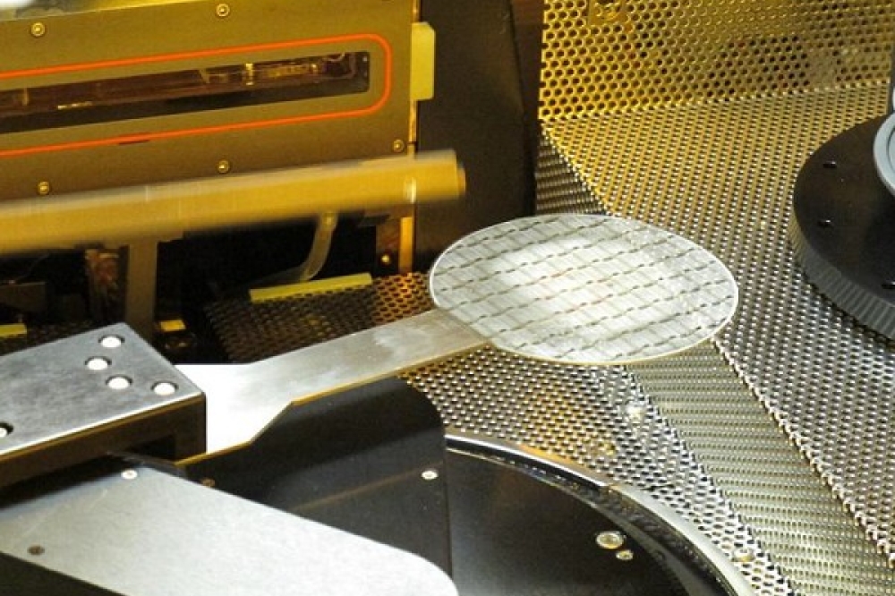
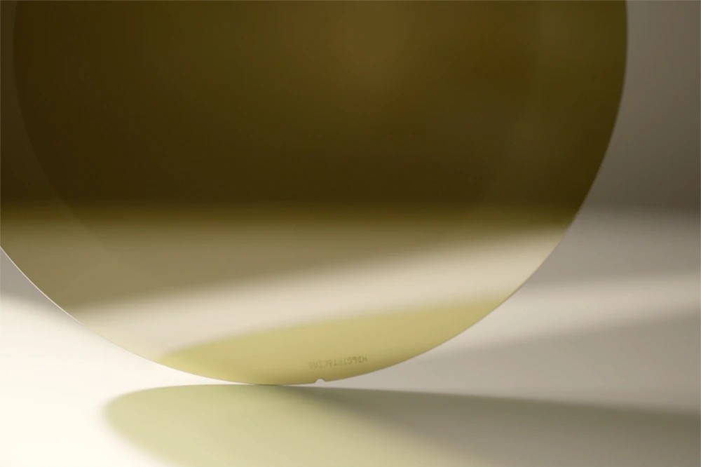
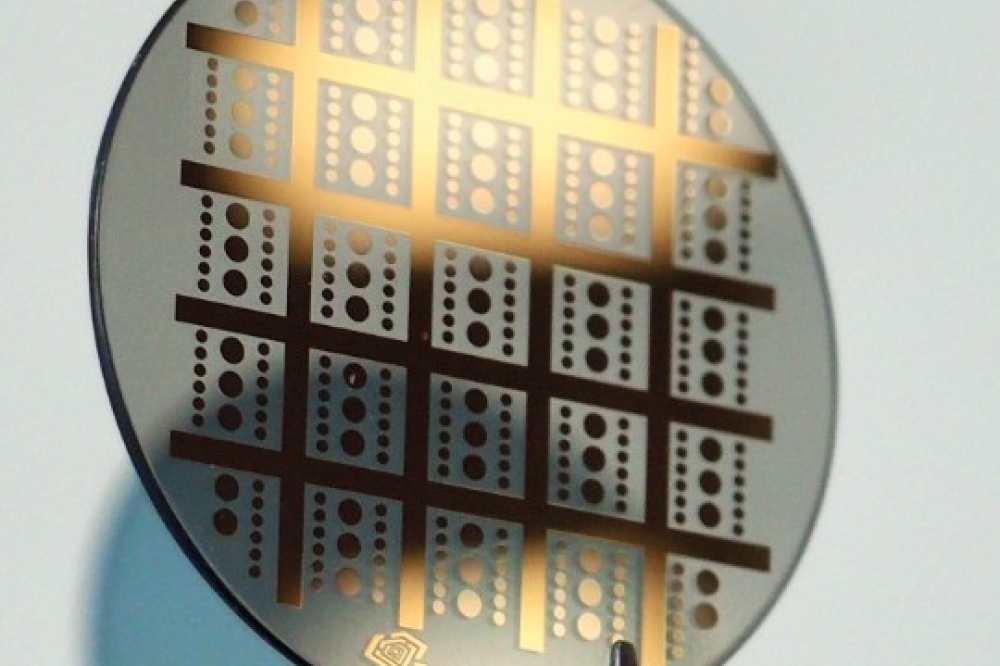
Main image: Schottky diodes on a diamond wafer, © Diamfab