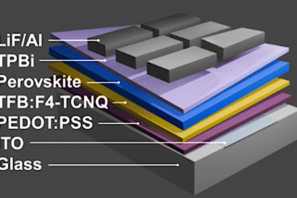
Producing high-quality hexagonal BN
The growth of high-quality hexagonal BN benefits from a sweet spot for nitrogen pressure that’s well beyond one atmosphere but far lower than that used to produce diamond.
BY BOHDAN SADOVYI, PETRO SADOVYI, SYLWESTER POROWSKI AND IZABELLA GRZEGORY FROM THE INSTITUTE OF HIGH PRESSURE PHYSICS POLISH ACADEMY OF SCIENCES, AND ANDRII NIKOLENKO FROM THE INSTITUTE OF SEMICONDUCTOR PHYSICS NATIONAL ACADEMY OF SCIENCES OF UKRAINE
Since the late 1990s, nitrides have grown in stature within the compound semiconductor community. They shot to prominence as the foundation for efficient LEDs that are now lighting our homes, offices and communities. That’s not the end of story, though, but rather the beginning. As well as a revolutionary light source, in the form of both the LED and the laser, nitride devices are playing an ever-increasing role in the power electronics and RF industries.
During the decades that have witnessed an increasing uptake of nitride devices, a miniaturisation of all semiconductor technologies has proceeded, in some cases down to the atomic scale. The discoveries of graphene, topological insulators and other novel materials have opened a whole new area, namely two-dimensional electronics. This new frontier has spurred the rediscovery of boron nitride (BN), a member of the family of III-N compounds that has much promise for modern electronics.

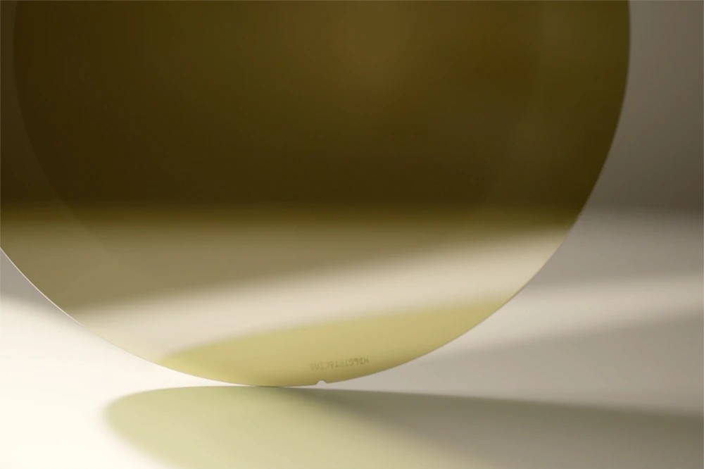
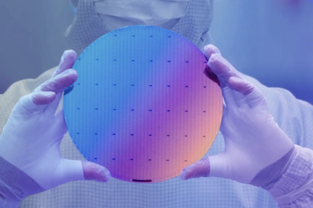
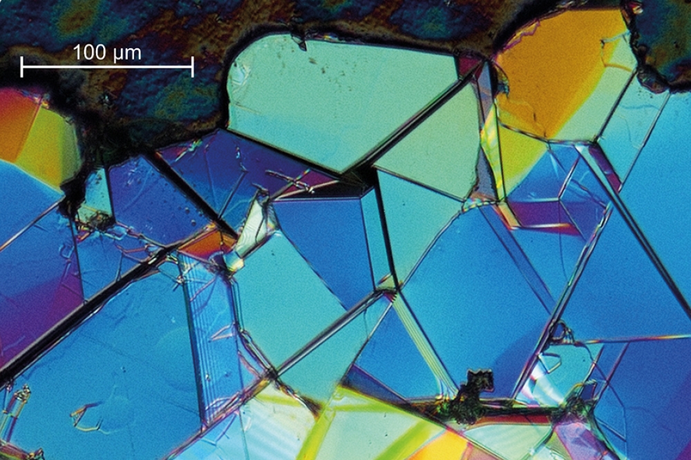
hBN flake obtained using pure nickel as the solvent
Of the many forms of crystalline BN, that with a hexagonal structure attracts particular interest for electronic applications. This form, referred to as hBN, is well established, having been widely deployed for many years. It has found use as a crucible material, in the form of sintered ceramics that benefit from its high thermal and chemical stability, and as a solid lubricant, thanks to its layered structure. Now new opportunities beckon, with hBN under investigation as a potential platform for 2D electronics and quantum technology.
Crystalline considerations
Like carbon, BN forms crystalline structures with different atomic configurations at different pressure-temperature conditions. At relatively low pressures, BN is thermodynamically stable in its hexagonal graphite-like structure. This form features monoatomic layers strongly bound in a honeycomb pattern, like graphene, and inter-bonded with weak van der Waals forces. However, while graphene and hexagonal BN have similarities in their crystalline form, they differ in electrical conductivity, with hBN behaving as a strongly insulating crystal.
This strongly insulating characteristic is to be expected, given that hBN has an incredibly wide bandgap of 6 eV. In monolayer hBN this gap is direct, but it shifts to indirect as the number of layers increases. Surprisingly, regardless of whether this material has a direct or indirect band gap, the UV optical emission produced by hBN is extremely efficient.
It is possible to exploit the insulating character of hBN. Employed in its two-dimensional form as very thin structures – they may have just a monoatomic layer – hBN can be deployed as an excellent insulator or tunnelling dielectric barrier in devices based on graphene and other 2D heterostructures. In these devices, incredibly thin layers of hBN boost performance.

Figure 1. A high gas pressure reactor with an internal diameter of 60
mm. (a) High-pressure chamber for pressures of up to 1.5 GPa. (b)
Graphite heater on alumina isolating tube. (c) High-pressure plug with a
crucible with thermocouples along its walls. (d) An illustration of a
high-nitrogen-pressure growth from solution approach used for GaN
crystallization (photo of real GaN single crystal is inserted on the
right-hand side).
Additional opportunities arise in hBN due to defects within the material. These imperfections, often regarded as a nuisance in compound semiconductors, enable very interesting physical systems that provide single-photon emitters, or centres hosting quantum spin states with a long coherence time. Such systems are needed as the bedrock for quantum technologies.
Single-crystal hexagonal BN
For both fundamental studies and the pursuit of new applications, it is critical to produce high-quality crystalline hBN, as this holds the key to uncovering its fascinating properties, as well as evaluating the predictability of theoretical models. Without access to a high-quality hBN crystal, the picture is disturbed by non-intentional defects, impurities, or strain if the crystal is deposited as an epitaxial layer on a foreign substrate.
Unfortunately, it is far from easy to grow crystalline hBN. Due to a melting temperature that exceeds 3000 °C, hBN, unlike silicon and GaAs, cannot be grown from its stoichiometric melt. Due to this limitation, two leading methods have emerged for the crystallization of hBN. One of them, developed by Takashi Taniguchi and co-workers at NIMS, Japan, involves very high pressures of 5 GPa or more, and metallic solutions, containing the likes of barium, magnesium and nickel. The alternative – proposed by Yoichi Kubota from NIMS and developed by James Edgar from Kansas State University – is based on growth on the surfaces of molten transition metal alloys containing boron, and involves a flow of nitrogen gas at atmospheric pressure. For both approaches, crystals are limited to the order of 1 mm in size – although this is sufficient for a reference material for fundamental research. Another concern is the very small thickness of the hBN crystals grown on metal surfaces under atmospheric N2 pressure.
Efforts have also been directed at growing thin layers of hBN on foreign substrates by CVD and MBE. The obvious, interesting choice of substrate for this work is highly oriented graphite, which has a similar structure – it has provided the foundation for growth of high-quality hBN layers.
It is clear that there are challenges in the crystallisation of hBN. This has motivated our team – a collaboration between the Institute of High Pressure Physics, Polish Academy of Sciences and the Institute of Semiconductor Physics, National Academy of Sciences of Ukraine – to develop a new approach to growing this exciting wide bandgap semiconductor.

Figure 2.The hBN growth process.
Nitrogen pressure – what for?
In stark contrast to GaN and InN, hBN does not require a high nitrogen pressure to suppress its decomposition at high temperatures. Consequently, this material can be crystallised from high temperature solutions under nitrogen at atmospheric pressure. However, this approach is not as easy as it may appear at first glance, because nitrogen has an incredibly low solubility in the metals that would to be used as a growth solution for hBN. According to a paper by Yoichi Kubota and co-workers from NIMS, nitrogen solubility in pure nickel at 1550 °C is as low as 0.0012 wt. percent.
Fortunately, the situation can be improved with relatively modest increases in nitrogen pressure. Recently, we have shown that it is possible to significantly enhance the nitrogen solubility in iron by increasing the free energy of nitrogen gas through compression. At atmospheric pressure and 1450 °C, only 0.5 at. percent of nitrogen can be dissolved in pure iron. Increase the nitrogen pressure to 1 GPa – that’s roughly 10,000 atmospheres – and the proportion of nitrogen that can be dissolved increases by over 20 times.
For high-temperature methods using atmospheric nitrogen pressure, the solubility of nitrogen in basic solutions, such as those formed by dissolving in nickel and iron, increases with additives that have a high affinity to nitrogen. For example, if pure nickel is replaced with the Ni-Cr eutectic, the solubility of nitrogen increases by 40 times. However, these additives are chemically active, complicating the growth of hBN. To avoid this, we have focused on the high N2 pressure approach to the crystal growth of hBN. Our expectation is that through the controlled increase of nitrogen solubility in molten metals, we will enhance the growth of hBN in the c-direction in the case of surface crystallisation, and enable the production of thicker crystals.
Our ultimate goal is to establish a new approach, where in contrast to crystallisation of hBN on metal surfaces, crystals will be grown in the solution volume. That’s mirroring the technique that we honed for the production of high-quality single crystals of GaN with dimensions of more than 1 cm (see Figure 1(d)). A driving force behind this particular methodology is the use of a temperature gradient, which enables controlled crystallisation at a constant temperature in a feed-seed configuration.

Figure 3. Results of hBN crystallization with Ni-Cr solution, at a N2
pressure of 0.1 GPa, in a temperature gradient: (a), cross-section of
the Ni-Cr-B-N ingot: CrN crystals are visible at the bottom part; (b),
general view of the upper part of the ingot: a large metallic droplet
emerged on the top (a very reproducible result); (c) the droplet covered
with transparent hBN crystals; (d) free-standing hBN crystals
exfoliated from the metal surface
Those of us at the Institute of High Pressure Physics, Polish Academy of Sciences, work within a department that is internationally renowned for its development of reactors for crystal growth that can be monitored with a high degree of precision (see Figure 1). These reactors are capable of accommodating gas pressures as high as 1-2 GPa, temperatures in excess of 1500 °C, and relatively high volumes, with internal diameters of 30 mm to 100 mm. Sets of thermocouples monitor the temperature within these reactors, allowing for precise control of temperature, temperature gradients and their changes over time. This level of control has held the key to establishing thermodynamic properties that have provided the foundation for the growth the first high-quality crystals of GaN thirty years ago. These GaN crystals, which have been extensively characterised, have been employed for homoepitaxy, thus opening this important field in GaN technology.
Initial experiments
We began investigating the growth of hBN by adopting the atmospheric pressure, high-temperature method pioneered by James Edgar. This approach involves forming a homogenised Ni-Cr eutectic mixture in an argon atmosphere at 1450 °C. Quickly building on this work we added some boron, replaced argon with nitrogen gas at a pressure of 0.1 GPa, and heated this system to 1450 °C to drive the dissolution of boron in the Ni-Cr melt. We established a temperature difference, varying from 1390 °C at the bottom of the metal ingot to 1450 °C at its top, and maintained this condition for 50 hours (see Figure 2 for an illustration of the crucible at the crystallisation phase).
These conditions led to very encouraging results regarding the growth of high-quality hBN. However, it’s not been easy to interpret what happened in the crucible. We observed: efficient growth of CrN crystals at the bottom of the crucible (see Figure 3(a)); at the top of the ingot, a large droplet depleted in chromium, and containing nickel, chromium, boron and nitrogen (see Figure 3(b)); and a surface of the droplet entirely covered with colourless, transparent crystals, identified as pure hBN (see Figure 3(c) and Figure 3(d)).
Our first crystals, which covered the metallic droplets, were fully transparent, colourless and featured mirror-like surfaces. According to energy-dispersive X-ray spectroscopy and X-ray diffraction, the hBN that we had formed had a single phase, with a c lattice parameter of 6.652 Å. The exfoliated hBN flakes, such as that shown in Figure 3(d), reached a size of a few to a few tens of mm2. These flakes featured domains with lateral dimensions between 50 mm and 200 mm, with borderlines well-oriented along directions of the hexagonal honeycomb lattice.
Using an optical microscope to inspect the c-plane surface of the hBN flake adjacent to the metallic droplet during growth revealed spirals and two-dimensional growth islands that are often intersected by borderlines, which may be overgrown cracks (see Figure 4). These findings suggest that at some stages of the process, the crystal grew as a whole, prior to cracking, due to geometrical reasons, such as solidification of the metal droplet.

Figure 4. hBN crystal grown from Ni-Cr solution at 0.1 GPa N2
pressure at 1450 °C. The growth hillock is visible in the central part,
proving that growth also takes place in the direction of the c-axis.
One of the implications of this particular growth morphology is that crystallisation on the c-plane of hBN probably proceeds from inside the solution. Note that this finding contrasts with the common interpretation of surface crystallisation of hBN, involving only lateral growth under constant availability of nitrogen from the gas phase. We are encourgaed by this, as it provides an opportunity to grow thicker platelets of hBN, thanks to the increased solubility of nitrogen in the growth solution.
We have also assessed the structural quality of our first hBN crystals with micro-Raman spectroscopy, with measurements at several points of the hBN flakes. In general, those spectra confirm a very high quality for our crystals, according to commonly accepted criteria. In particular, the strong and narrow E2g Raman lines, with a full-width-at-half-maximum below 8 cm-1, demonstrate the high perfection and uniformity of our hBN crystals (see Figure 5). It is only possible to obtain narrower peaks by turning to isotopically pure boron and nitrogen for crystallisation, an approach adopted by Edgar and co-workers.

Figure 5. MicroRaman spectra of hBN.
Next steps
Our initial findings show that adding chromium to nickel significantly disrupts the Ni-Cr-B-N growth system under a N2 pressure of 0.1 GPa and temperatures ranging from 1390 °C to 1450 °C.
We have been able to observe excellent growth in the temperature gradient of CrN crystals, with hBN crystals forming solely on the metal surface. This led us to embark on a new set of experiments, involving the removal of chromium from the system, replaced by N2 under high pressure. This change provides an efficient source of nitrogen, which can dissolve in molten nickel or other selected solvents.
Using this approach, we have investigated hBN growth using a relatively low pressure of 0.1 GPa and a slow cooling stage, in the 1450 °C – 1350 °C temperature range. These conditions result in similar surface crystallisation to our previous work with Ni-Cr. Again, transparent and colourless flakes are exfoliated from the metal surface. We have found that the dimensions of the individual crystalline hBN domains varies according to the initial concentration of boron added to the solution. These domains can be as small as 25 mm and 50-100 mm for 4 wt. percent and 2 wt. percent of boron, respectively.
We can conclude from this work that there is probably enhanced hBN nucleation on the metal surface, which is detrimental for growing large hBN crystals by this method. Similar to growth at atmospheric pressure and high temperatures, it is crucial to establish equilibrium conditions for the BN-solvent system (the liquidus curve). Doing so ensures a proper start to the supersaturation stage, by either slow cooling or the application of a temperature gradient
Our initial experiments have determined that the enhanced nitrogen solubility, resulting from high pressure, does not in itself hold the key to obtaining thicker hBN crystals. We have also discovered that it’s essential to develop a method for supplying nitrogen to the volume of the solution during the crystallisation process. This represents one of the subsequent phases in our ongoing research, focused on developing a more effective method for the crystallisation of hBN, which is without doubt a significant and intriguing material.