Taking the power of the InP PCSEL to new highs
A partnership from Japan that includes the group that invented the photonic crystal surface-emitting laser (PCSEL) claims to have smashed the output power for this class of device at 1550 nm.
This team’s InP-based laser, produced by a partnership between its pioneers at Kyoto University and engineers at Sumitomo Electric Industries, is capable of delivering a continuous output power of 300 mW. Prior to this success, the most powerful PCSELs emitting at around 1.55 mm were only capable of emitting 100 mW under pulsed operation.
The PCSEL is renowned for its single-mode operation, high optical power and high-quality narrow-divergence angle beam – and more powerful versions emitting around 1.55 mm are attractive sources for lidar, material processing and optical communication.
“We believe that 300 mW [PCSELs] can already meet requirements for some practical applications,” remarked Kyoto University’s Susumu Noda, who attributes the record-breaking output power of the team’s PCSEL to advances in design and processing.
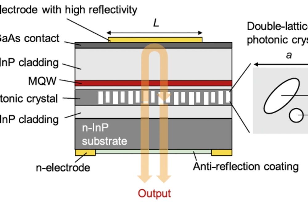
“Our double-lattice photonic crystal design is optimised for the 1550 nm wavelength, based on our extensive experience with GaAs-based and InP-based PCSELs,” said Noda. “Additionally, our well-controlled etching and regrowth processes result in minimal damage, thereby reducing optical losses.”
Fabrication of the team’s PCSEL began with the growth of an epitaxial stack by MOCVD, followed by the formation of a photonic crystal structure, using electron-beam lithography and dry etching. Overgrowth of an InP spacer layer encapsulated air holes, prior to addition of an active region featuring four InGaAsP quantum wells, followed by a p-type InP cladding layer and a heavily p-doped GaInAs contact layer. By taking this approach, the team avoided any chance of damaging the active layer.
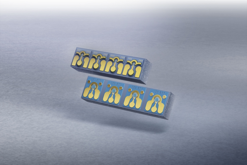
To complete the fabrication of their PCSEL, Noda and colleagues added electrodes. Their n-type electrode, which defines the size of the device and features a circular window through which the light is emitted, has a diameter of 200 mm. As well as injecting carriers, the p-type electrode serves as a backside reflector that enhances slope efficiency.
The InP-based PCSEL features a double-lattice photonic crystal structure, employed to realise high-power single-mode operation, that combines small circular holes with those that are larger and elliptical.
Measurements revealed a room-temperature maximum output power of 318 mW, realised at a wall-plug efficiency of 17.3 percent. At this temperature the threshold current is 230 mA, and the threshold current density 0.73 kA cm-2. The latter value is only a little higher than that of 0.67 kA cm-2, associated with the threshold current density of the team’s 1300 nm PCSELs. The team attribute this small increase in threshold current with wavelength to a larger intrinsic loss, and an increase in Auger recombination.
The team has recorded the room-temperature spectral emission of its latest PCSEL using a drive current of 1770 mA, corresponding to the peak output power. This measurement confirmed single-mode emission, peaking at 1564 nm, and provided a value for the full-width-at-half-maximum of less than 0.02 nm, which is the resolution of the analyser.
Values for the side-mode suppression ratio were measured for drive currents ranging from below 1000 mA to more than 2000 mA, and for temperatures from below 20 °C to 60 °C. In all cases, the side-mode suppression ratio exceeded 60 dB.
Noda and co-workers have also investigated the high level of stability of the single-mode operation of their PCSEL, with calculations attributing this asset to a large threshold gain margin, as well as a moderately weakened in-plane optical coupling of the photonic crystal structure.
According to Noda, the next goals for the team are to improve their designs, including the photonic crystal, and realise watt-class operation.
Pictured above : The double-lattice photonic crystal played a vital role in increasing the output power of 1.55 µm PCSELs.
Reference
T. Aoki et al. Appl. Phys. Express 17 042004 (2024)