KAUST team pioneers In₂O₃ TFT stack
A team of researchers at King Abdullah University of Science and Technology (KAUST) led by Saravanan Yuvaraja and Xiaohang Li has made a breakthrough in semiconductor technology, with the vertical integration of thin-film In2O3 transistors.
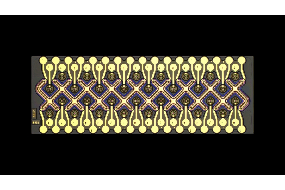
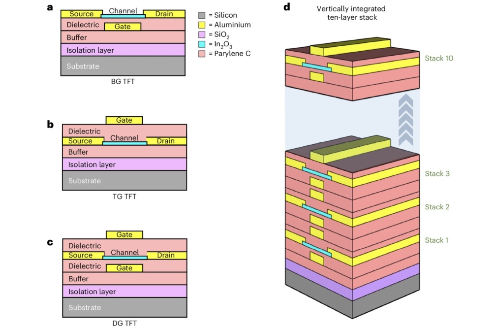
Published by Nature Electronics, the study shows a ten stack of nanometer-thin In2O3 transistors on a Si/SiO2 wafer. Unlike traditional planar transistor arrangements, the researchers say, this vertical stacking technique maximises wafer space, significantly enhancing performance efficiency and scalability.
The fabrication process began with the deposition of In2O3 TFTs at room temperature, ensuring compatibility with existing CMOS processes. Parylene-C was used as both the buffer and dielectric material due to its superior insulating properties and ease of processing.
The team sequentially deposited ten layers of In2O3 TFTs, comprising 72 functional layers, including metal electrodes and parylene-C layers. This meticulous patterning and deposition technique ensured precise alignment and optimal electrical performance.
The dual-gate In2O3 TFTs demonstrated a maximum field-effect mobility of 15 cm²/V·s, a subthreshold slope of 0.4 V/dec, and a current on/off ratio of up to 10⁸. These metrics are crucial for low power computing and mobile devices, where efficiency and speed are of paramount importance.
By integrating dual-gate transistors at different levels within the stack, the researchers created unipolar inverter circuits with a signal gain of approximately 50 and wide noise margins. The dual-gate configuration also allowed for fine-tuning of the inverters, achieving symmetric voltage transfer characteristics and optimal noise margins.
The team believes this achievement sets a new benchmark in 3D stacked transistors, highlighting the potential for creating scalable, high-density integrated circuits. The approach addresses key challenges in the field, such as low power density and high-temperature bonding, by using a room-temperature process.
Looking ahead, the KAUST team plans to refine their fabrication techniques further and explore new materials and configurations to enhance the performance and reliability of stacked transistors.
The potential applications of this technology range from internet of things to edge AI operations.
Pictured above: a–c, Two-dimensional and 3D schematic representations of bottom gate BG (a), top gate TG (b) and dual gate DG (c) transistors. d, 3D schematic representation of 10 stack dual gate transistors on an Si/SiO2 substrate.
'Three-dimensional integrated metal-oxide transistors' by Saravanan Yuvaraja et al: Nature Electronics (2024)