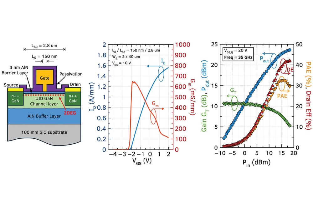
BN transistor has 'superlative properties'
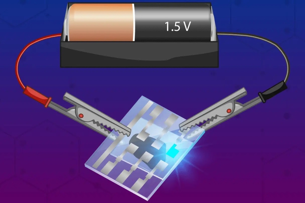
MIT researchers and colleagues have used the 2D compound semiconductor boron nitride (BN) to build a transistor that has "superlative" properties. The work 'Ultrafast high-endurance memory based on sliding ferroelectrics' was reported in a recent issue of Science.
In 2021, a team led by MIT physicists created an ultrathin BN-based ferroelectric material; one where positive and negative charges separate into different layers. At the time they noted the material’s potential for applications in computer memory and much more. Now the same core team and colleagues — including two from the lab next door — have built a transistor with the material.
Although the team’s results are based on a single transistor in the lab, “in several aspects its properties already meet or exceed industry standards” for the ferroelectric transistors produced today, says Pablo Jarillo-Herrero, the Cecil and Ida Green Professor of Physics, who led the work with professor of physics Raymond Ashoori. Both are also affiliated with the Materials Research Laboratory.
The new transistor can switch rapidly between positive and negative charges on nanosecond time scales. It is also extremely tough: after 100 billion switches it still worked with no signs of degradation. And because the material is so thin, it could allow for much denser computer memory storage and more energy-efficient transistors, say the researchers.
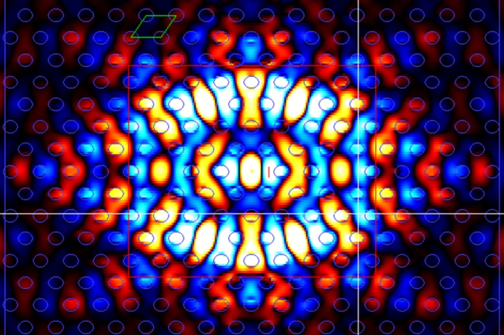
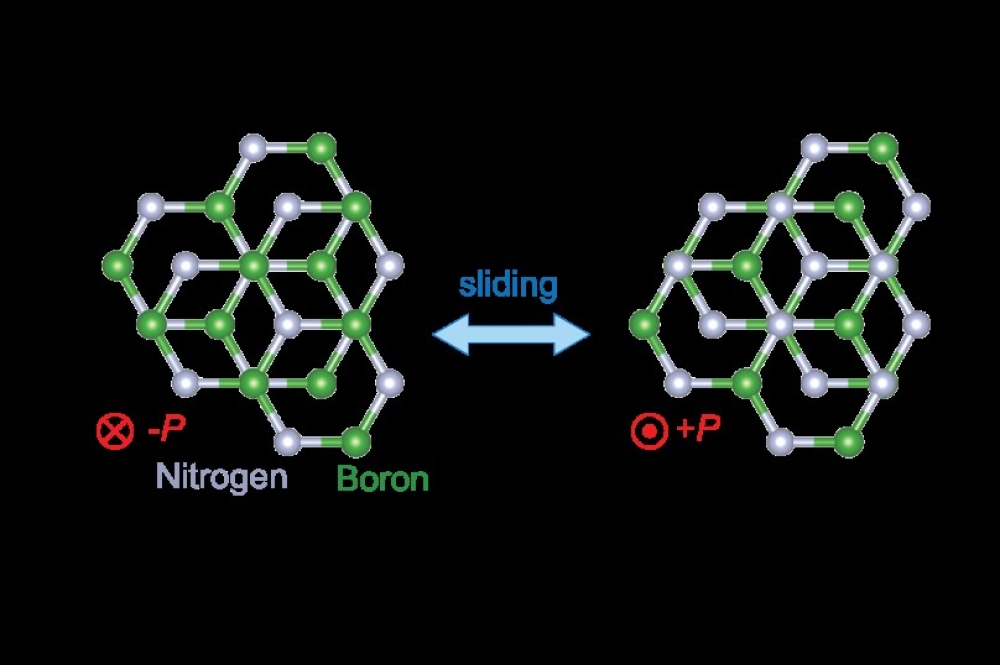
The new ferroelectric material reported in 2021 is based on atomically thin sheets of boron nitride that are stacked parallel to each other, a configuration that doesn’t exist in nature. In bulk BN, the individual layers of BN are instead rotated by 180 degrees.
It turns out that when an electric field is applied to this parallel stacked configuration, one layer of the new BN material slides over the other, slightly changing the positions of the boron and nitrogen atoms.
“So the miracle is that by sliding the two layers a few angstroms, you end up with radically different electronics,” says Ashoori. The diameter of an atom is about 1 angstrom.
“Nothing wears out in the sliding,” Ashoori continues. That’s why the new transistor could be switched 100 billion times without degrading. Compare that to the memory in a flash drive made with conventional materials. “Each time you write and erase a flash memory, you get some degradation,” says Ashoori. “Over time, it wears out, which means that you have to use some very sophisticated methods for distributing where you’re reading and writing on the chip.” The new material could make those steps obsolete.
Challenges remain. For example, the current way of producing the new ferroelectrics is difficult and not conducive to mass manufacturing. “We made a single transistor as a demonstration. If people could grow these materials on the wafer scale, we could create many, many more,” says co-first author Kenji Yasuda, now an assistant professor at Cornell University. He notes that different groups are already working to that end.
Concludes Ashoori, “There are a few problems. But if you solve them, this material fits in so many ways into potential future electronics. It’s very exciting.”
This work was supported by the US Army Research Office, the MIT/Microsystems Technology Laboratories Samsung Semiconductor Research Fund, the US National Science Foundation, the Gordon and Betty Moore Foundation, the Ramon Areces Foundation, the Basic Energy Sciences program of the US Department of Energy, the Japan Society for the Promotion of Science, and the Ministry of Education, Culture, Sports, Science and Technology (MEXT) of Japan.