Raising the bar for power amplification

The performance of GaN-based amplifiers operating in the X- and Ka-bands record new highs through the introduction of an AlN buffer.
BY YANG LING, HAO LU, BIN HOU, FUCHUN JIA, XIAOHUA MA AND YUE HAO FROM XIDIAN UNIVERSITY
In communication infrastructure and radar systems, there is much demand for more powerful power amplifiers (PAs). By increasing the strength of signal through greater amplification, more powerful PAs can open the door to improving the design and the capability of wireless networks, and the resolution and reach of radar.
A compelling approach to increasing the power of the PA is to enhance the buffer design. One option is to switch to compensation doping in the GaN buffer – this boosts the resistance of this layer, leading to a reduction in RF insertion loss, and in turn a hike in the operating voltage of the GaN device.

Figure 1. Improvements in RF performance are realised by introducing an iron-doped AlN buffer (a). This design is superior to the conventional iron-doped GaN heterostructure (b). Note that these illustrations are not to scale.
However, while this approach sounds easy, success is far from trivial. Our team from Xidian University initially tried to succeed in this manner, with efforts beginning by exploring compensation doping in GaN buffers. Through the integration of deep-level impurities such as either iron or carbon, we aimed to significantly increase the buffer’s resistivity, and ultimately the breakdown and power characteristics of the PA. But we came up against a number of hurdles, including the unintended introduction of carbon-related buffer traps and an iron-related doping tail effect – both threaten to degrade device performance. In addition, we found our quest for optimal material quality to be hampered by limitations in thermal management, originating from the thickness of the doped GaN buffer layer.
In response to these challenges, we switched to an AlN buffer. It’s a formidable solution: boasting a high thermal conductivity and an ultra-wide bandgap, this form of buffer has emerged as a beacon of innovation, poised to redefine the standards of PA design. We have deployed this buffer as the foundation for recording-breaking levels of amplification in the X- and Ka-bands.

Figure 2. Secondary ion mass spectrometry provides profiles of the iron, silicon and carbon elements in GaN/AlN/SiC hetero-structures.
Inserting AlN buffers
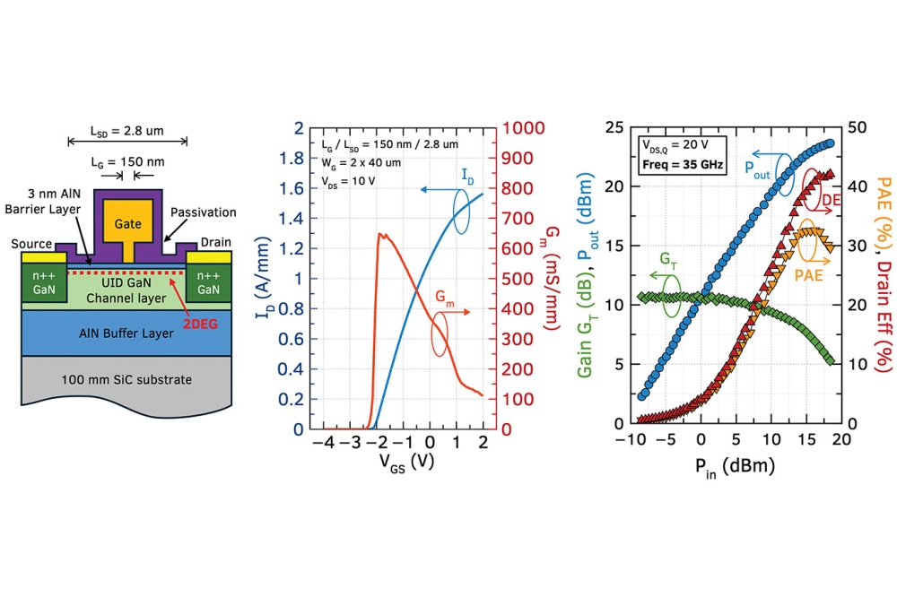
Fabrication of these devices began by loading a 75 mm semi-insulated SiC substrate into an MOCVD reactor and growing a ultrathin AlN buffer layer at high-temperature, followed by an unintentionally doped GaN channel layer, an AlN insert layer, and a Al0.25Ga0.75N barrier layer (see Figure 1).
To uncover the doping profiles in this design, we scrutinised our epitaxial structure with secondary ion mass spectrometry (see Figure 2). This technique revealed a sharp profile for the iron concentration at the interface between the undoped GaN and AlN, indicating the elimination of the iron-doping tail effect, thanks to incorporation of the AlN buffer.
We have investigated the interface between the SiC substrate and AlN buffer with high-angle dark-field scanning transmission electron microscopy and energy-dispersive X-ray spectrometry (see Figures 2 and 3). This pair of techniques revealed a continuous sharp boundary, as well as no element inter-diffusion between the AlN buffer and the substrate.
To produce GaN-based HEMTs with two types of buffer layer structures from our epiwafers, we began by adding an alloyed source/drain ohmic contact, prior to deposition of a 120 nm SiNx passivation layer. Subsequent electrical isolation resulted from planar nitrogen-ion implantation, followed by the removal of SiNx passivation under the gate stem and the formation of Ni/Au gate electrodes for the Schottky contact.
Devices with two types of epitaxial heterostructure were produced using the same process flow and device geometry. These HEMTs have a 0.5 µm gate length and a 3.1 µm gate-drain spacing. We have also fabricated transistors for millimetre-wave applications – that’s frequencies of more than 30 GHz – by scaling down the AlN buffer device using the same process platform to produce a HEMT with a 150 nm gate length.

Figure 3. Transmission electron micrograph of the iron-doped AlN buffer structure.
Better breakdown
By switching from GaN to AlN, our buffer has a higher thermal conductivity that eradicates heat dissipation issues in this region of the device. The AlN buffer also improves channel conductivity and transport properties by eliminating the iron doping-tail effect.
These benefits of the AlN buffer are seen in our measurements of DC and small-signal characteristics. Thanks to a high field-effect mobility, we see higher values for the transconductance in our AlN buffer device, alongside superior values for the cut-off frequency (fT) and the maximum oscillation frequency (fmax). These findings have been drawn from our studies of small-signal characteristics for devices with AlN and GaN buffers, operating under a drain-source voltage of 10 V.
We have recorded values for fT and fmax of 29.1 GHz and 50.7 GHz, respectively, for our HEMTs with an AlN buffer. These devices, which have a breakdown voltage that is linearly related to the gate-drain spacing, have a breakdown voltage more than 100 V higher than that of variants with the conventional GaN buffer. According to plots of breakdown voltage as a function of source-drain distance, our devices have an average breakdown field of 0.87 MV cm-1. We have also measured the double-pulsed current-voltage characteristics of HEMTs with an AlN buffer, and those with a GaN buffer. These plots show that the introduction of the AlN buffer effectively suppresses current collapse, and trims the current-collapse ratio by nearly 13.2 percent.
Encouraging results have also been obtained for our scaled-down device that’s targeting the Ka-band. This 150 nm HEMT has a breakdown-field of 0.76 MV cm-1, and values for fT and fmax of 50 GHz and 145 GHz, respectively. Meanwhile, simulations suggest that the channel temperature is lower with an AlN buffer, than a GaN buffer, and RF loss is significantly reduced.

Figure 4. Comparison of X-band power results from various reports for (a) output power (Pout) versus power added efficiency (PAE); (b) Pout versus drain-source voltage (VDS).
Record-breaking power densities
The X-band is renowned for electromagnetic waves with strong reflectivity and a short wavelength. Due to these traits, the X-band is widely used for wireless communication, as well as a number of other applications. For wireless links, the PA’s power performance is crucial, as it directly affects the operating performance. The PA must deliver sufficient power to ensure that signals are transmitted effectively over long distances, while offering a high level of efficiency that enables minimal heat generation and power consumption. Amplifiers also need to provide good linearity, as this ensures signal integrity and minimises distortion.
To perform large-signal power characterisation at 10 GHz in pulsed mode, we employed an active load-pull system. Operating in the X-band, our devices produced an output power of 33.1 W mm-1, and under optimum output power tuning, a peak power-added efficiency of 55.1 percent. Meanwhile, under optimum power-added efficiency tuning, our HEMTs delivered a maximum power-added efficiency of 62.9 percent, realised at an output power density of 32.5 W mm-1.
For PAs, the two key characteristics for benchmarking are the output power as a function of power-added efficiency, and the output power as a function of drain-source voltage. Using these criteria, we benchmarked our HEMTs against state-of-the-art results (see Figure 4). This exercise shows that our design achieves high efficiency at high output power density, and the output power of this portfolio of devices tends to increase linearly with increasing drain-source voltage, even within a wide drain voltage range, spanning 10 V to 130 V.

Figure 5. (a) Active load-pull test results at Ka-band for the scaled-down HEMT. (b) Benchmark of millimetre-wave power performance from various reports for Pout versus VDS.
We have also studied our devices that amplify in the Ka-band, which ranges from 26.5 GHz to 40 GHz. This band is used for satellite communication, including high-speed satellite broadband, as well as ground wave tracking, collecting weather information and visible/infrared imaging. Compared with the X-band, wavelengths are shorter, enabling higher resolution – and there is the opportunity for broadcasting services to cover larger geographical areas. While operational power performance is vital for any amplifier, in higher frequency bands like the Ka-band, it is also crucial to handle amplified signals without introducing excessive noise or distortion. This implies the need for robust thermal management solutions and a low RF loss, to ensure the clarity and quality of the amplified signal.
Scaling our devices to a 150 nm gate length so that they operate in the Ka-band leads to a record power density of 14.4 W mm-1 and a maximum power-added efficiency of 48 percent. We benchmarked this device, considering output power as a function of the drain-source voltage. For this evaluation, we determined that for our devices the power-voltage ratio – a measure of the modulation ability of the drain-source voltage on the output power – is 0.52 W mm-1 V-1. According to this metric, our devices even outperform N-polar GaN devices, with further gains promised by increasing the drain-source voltage and employing a strong-polarisation thin-barrier design in the Ga-polar material system. This shows that devices with the AlN buffer also have plenty of potential for millimetre-wave applications.
Further reading / Reference
L. Yang et al., “Record Power Performance of 33.1 W/mm with 62.9% PAE at X-band and 14.4 W/mm at Ka-band from AlGaN/GaN/AlN:Fe Heterostucture,” 2023 International Electron Devices Meeting (IEDM), San Francisco, CA, USA, 2023, pp. 1-4