News Article
SemiQ expands high-performance power module family
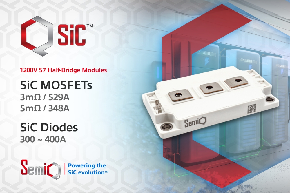
High-performance 1200V SiC power modules offer optimized solutions for new designs and improved performance in legacy applications
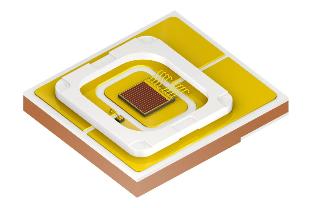
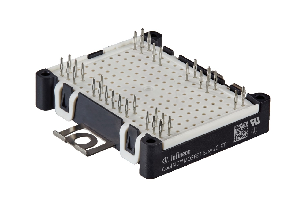
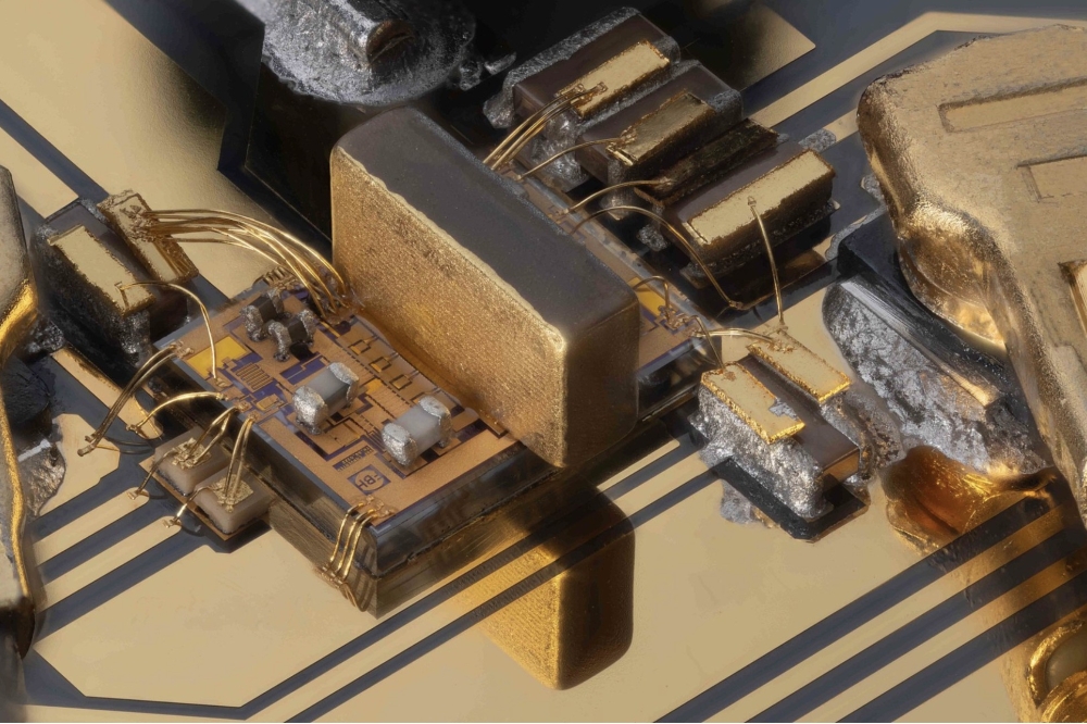
SemiQ Inc, a designer, developer, and global supplier of superior silicon carbide (SiC) solutions for ultra-efficient, high-performance, and high-voltage applications, has announced the addition of an S7 package to its QSiC™ family of 1200V, half-bridge MOSFET and Schottky diode SiC power modules. The parts further enhance design flexibility for power engineers by providing compact, high-efficiency, high-performance options for new designs while supporting drop-in-replacement in legacy systems that require more efficient operation.
The new package addresses the size, weight and power requirements of demanding applications ranging from induction heaters, welding equipment and uninterruptible power supplies (UPS) to photovoltaic and wind inverters, energy storage systems, high-voltage DC-DC converters and battery charging systems for electric vehicles (EVs). As well as the compact form factor of the modules themselves, high-efficiency, low-loss operation helps to reduce system heat dissipation and supports the use of smaller heatsinks.
“Our aim is to provide a comprehensive portfolio of SiC technologies that allow designers to optimize the efficiency, performance and size of today’s demanding applications,” says Dr. Timothy Han, President at SemiQ. “Adding new package option to our 1200V QSiC MOSFET and SiC diode module families further extends the choices available to designers who need to create completely new applications or who are looking to upgrade legacy systems without significant redesign.”
Crafted from high-performance ceramics, SemiQ’s modules achieve exceptional performance levels and support increased power density and more compact designs - especially in high-frequency and high-power environments.
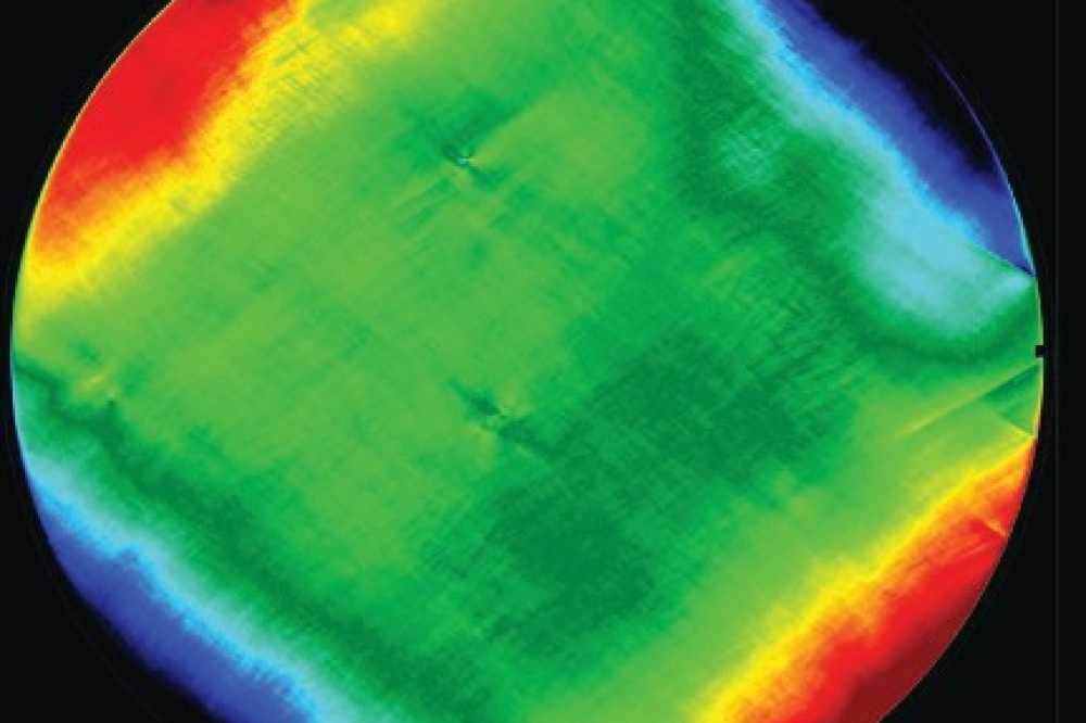
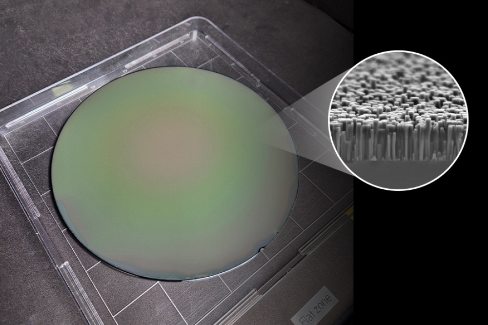
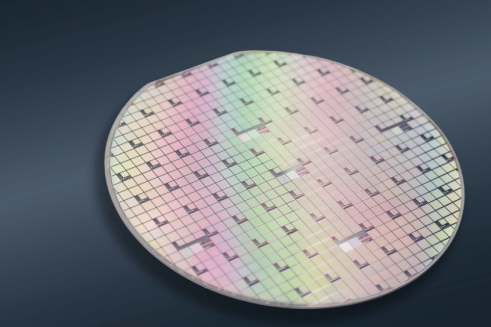
To guarantee a stable gate threshold voltage and premium gate oxide quality for each module, SemiQ conducts gate burn-in testing at the wafer level. In addition to the burn-in test, which contributes to mitigating extrinsic failure rates, various stress tests - including gate stress, high-temperature reverse bias (HTRB) drain stress, and high humidity, high voltage, high temperature (H3TRB) - are employed to attain the necessary automotive and industrial grade quality standards. All parts have undergone testing surpassing 1400V.