A new milestone in 2D layer-tronics?
A new study published in Nano Letters by researchers led by Singapore University of Technology and Design (SUTD), may help address the challenge of integrating ultrathin 2D transistors and interconnects without sacrificing contact performance.
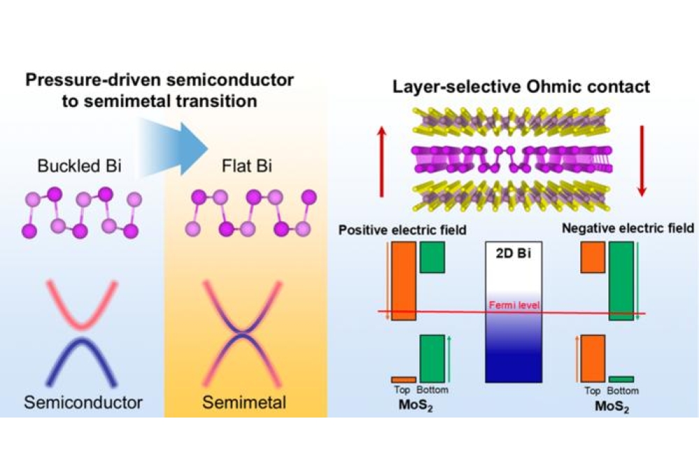
Using state-of-the-art density functional theory (DFT) simulations, they showed that when a single layer of the semiconductor bismuth is sandwiched between two layers of the 2D compound semiconductor MoS2, the atoms reorganise from a slightly corrugated (or buckled) structure into a perfectly flat one.
This structural flattening has dramatic electronic consequences, according to the team: it eliminates the energy band gap and allows electrons to move freely, turning the material metallic.
“Once the bismuth sheet becomes completely flat, the electronic states overlap, and the material suddenly conducts electricity like a metal. The transformation is fully driven by mechanical pressure,” said Shuhua Wang, a postdoctoral research fellow at SUTD.
This effect, which is in sharp contrast to the semiconducting character of bismuth predicted by decades of theoretical studies and previous experiments on freestanding monolayers, was reported earlier 2025 in a landmark Nature paper.
The newer research in Nano Letters has shown why confined bismuth conducts electricity when its unconfined counterpart does not.
By linking pressure, structure, and electronic behaviour, the team has demonstrated that van der Waals squeezing flattens the atomic lattice of bismuth, thus triggering the structural and electronic transition needed for metallicity.
The researchers have further proposed a MoS2-Bi-MoS2 trilayer heterostructure, where the atomically thin bismuth acts as a metallic bridge sandwiched between two semiconducting layers. Their simulations reveal a striking asymmetry: one MoS2 layer forms a low-resistance (Ohmic) contact with the metallic Bi, while the other forms a higher-resistance (Schottky) barrier.
By applying an external electric field perpendicular to the stack, the team showed that this Ohmic contact can be switched between the top and bottom layers, thus allowing electrical current to be steered between layers on demand.
They believe this mechanism, termed a layer-selective Ohmic contact, marks a new milestone in 2D electronics. It generalises the familiar metal–semiconductor interface into a layer-dependent, field-controllable contact – the essence of layertronics, a device concept that exploits the layer degree of freedom in 2D materials for data processing and storage.
“Traditional circuits are wired once and fixed forever,” said Yee Sin Ang, the project lead at SUTD. “In MoS2-Bi-MoS2 trilayer heterostructure, we can reconfigure where the current flows simply by tuning an electric field. That means the same device can perform multiple functions without any physical rewiring. It’s a key step toward reprogrammable, energy-efficient nanoelectronics.”
The team says this ability to fine-tune contact behaviour via mechanical or electrical fields provides a powerful, sustainable pathway toward the next generation of flexible, low-power, and reconfigurable computing chips.
References
Shuhua Wang et al; Nano Letters 2025 25 (40)
Zhao, J., Li, L., Li, P. et al; Nature 639, 354–359 (2025)