Broadening the nitride palette with AlYN
AlYN provides a promising material for pioneering sustainable high-performance applications and green technologies.
BY STEFANO LEONE, ISABEL STREICHER, PATRIK STRAŇÁK AND LUTZ KIRSTE FROM FRAUNHOFER IAF, FREIBURG,GERMANY
In today’s digitally connected society, characterised by the relentless demand for high-energy data computing that’s needed to power artificial intelligence (AI) applications, one key question is this: What must be done to keep up with the pace? Reflecting on this at the recent World Economic Forum Annual Meeting in Davos, OpenAI’s CEO, Sam Altman, issued a poignant warning, leaving no-one in any doubt that the future of AI hinges upon breakthroughs in energy efficiency, essential for accommodating the escalating demands for power consumption. Altman’s cautionary note is resonating deeply within the tech community, sparking a critical dialogue on the need for innovation in energy-efficient computing.
A new way of thinking is needed to ensure success on this front. Traditionally, efforts have focused on increasing power capacity to meet burgeoning computational requirements. Now, though, there is a need to shift to optimising existing technologies for efficiency. This paradigm shift, promoting the value of sustainability, is particularly pertinent in compound semiconductor materials, where advances in materials science are already unlocking new possibilities for enhancing performance while minimising energy consumption.

Scientists Lutz Kirste, Isabel Streicher and Stefano Leone from
Fraunhofer IAF, Freiburg, discuss on the stability of AlYN’s wurtzite
crystal structure and the challenges posed by cubic inclusions,
highlighting ongoing efforts to overcome material hurdles and advance
semiconductor technology.
One notable innovation in this regard is the development of AlYN, a novel nitride, by our team at the Fraunhofer Institute for Applied Solid State Physics IAF in Freiburg, Germany. Grown by MOCVD, AlYN holds immense promise as a key enabler in more efficient digital communication and energy-efficient computing.
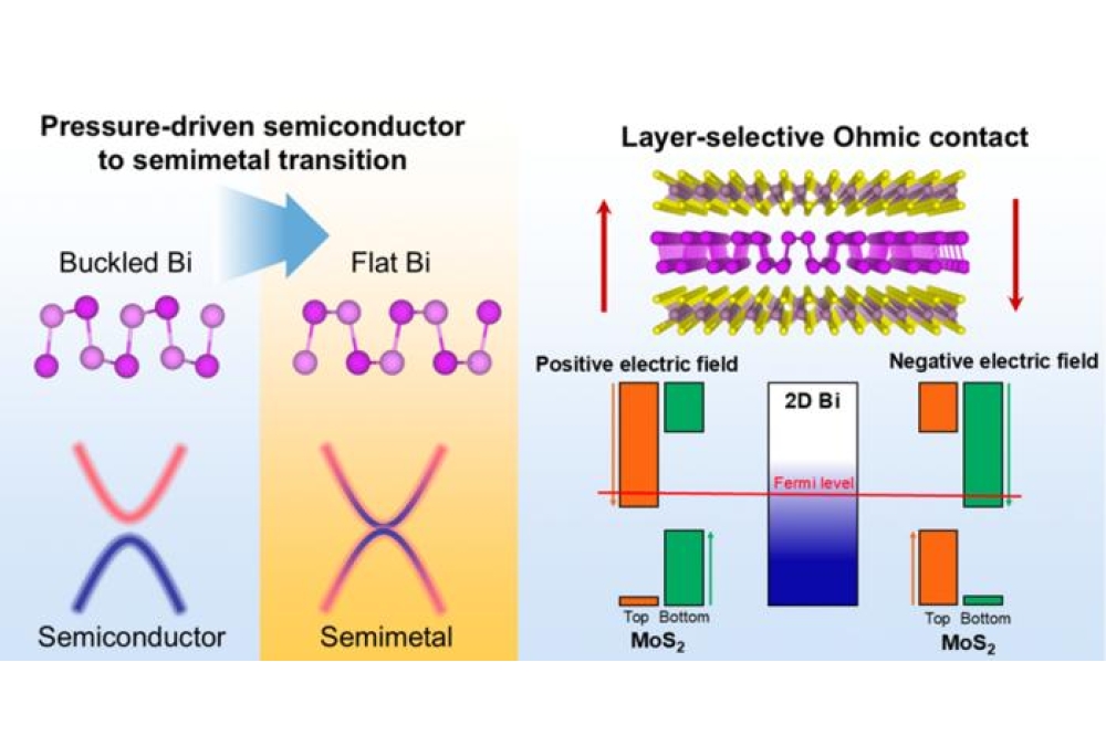
We are not the only trailblazer of this nitride. Work by Zetian Mi’s group at the University of Michigan has demonstrated that AlYN exhibits ferroelectric properties, akin to its counterpart, AlScN. This discovery opens up exciting avenues for exploring AlYN’s potential in novel applications, including non-volatile memories.
Within the worldwide research community, efforts to explore the use of AlYN for fabricating HEMTs are ongoing. While these transistors are still to be realised, significant strides have been made in demonstrating the epitaxial heterostructure necessary for their fabrication. Both MBE and MOCVD techniques have been employed to grow epitaxial AlYN/GaN heterostructures, showcasing the feasibility of integrating AlYN into HEMTs.
It should be noted that while AlYN’s ferroelectric nature provides potential for non-volatile memory, there has been no conclusive evidence of its functionality in this capacity. Nevertheless, ongoing research endeavours are diligently exploring the suitability of this novel nitride for non-volatile memory applications, propelled by its tantalising material properties and potential benefits for energy-efficient computing.

Figure 1. Temperature-dependent Hall measurement of the Al1-xYxN/GaN heterostructure with a value for x of 0.082. (a) Electron density (ns), (b) sheet resistance (Rsh)
and (c) mobility (µ). Calculated background residual impurity
scattering (BRI), interface roughness scattering (IFR), acoustic phonon
scattering (AP) and polar optical phonon scattering (POP) limited
mobilities are indicated.
Unveiling the potential of AlYN
Back in 2019, we realised a significant milestone, cultivating the first AlScN by MOCVD. This provided a pivotal moment in our journey to producing AlScN, which is blessed with exceptional physical properties that could revolutionise various sectors, from digital communication to power conversion. This nitride is renowned for its prowess in enhancing the performance of GaN-based HEMTs, an appeal that’s captivating the interest of researchers worldwide.
Surrounded by the fervour associated with AlScN, last year many delegates experienced an unexpected twist at the ICNS conference in Fukuoka, Japan. Sandwiched between a plethora of discussions centred on AlScN, our team had the chance to present not on AlScN, but AlYN. While some of the researchers at the conference might have thought that there had been a typographical error, it was actually the culmination of our pioneering efforts in semiconductor alloys – AlYN had entered the spotlight.
The genesis of our fascination with AlYN traces back to 2019, following our success with AlScN. This rationale was multifaceted: AlYN, stable in the wurtzite phase with higher yttrium concentrations, boasts distinct advantages over its counterparts. Notably, AlYN demands a lower yttrium content than scandium to realise lattice-matching with GaN, enabling enhanced performance and reliability. This alignment with GaN may offer many benefits, including a superior HEMT durability and the alleviation of constraints in layer thickness, crucial for ferroelectric applications in non-volatile memories.
Promoting the direction of our research are discussions surrounding the scarcity of scandium. This encouraged us to pivot our attention to yttrium, an abundant alternative coursing through the Earth’s crust. The accessibility of this transition metal, coupled with a significantly lower cost than scandium, makes it an enticing prospect for industrial applications. Yet, as with any innovation, we embarked on our efforts with a shadow of scepticism lingering over us: Would yttrium’s propensity for oxidation prove a hindrance?

In the X-ray diffraction lab at Fraunhofer IAF, Freiburg, scientists
Mario Prescher and Nadine Brückner meticulously analyse the
crystallographic structure of AlYN layers, providing essential data for
optimising material quality and understanding its relationship with
underlying GaN layers.
Back to 2012
Note that we are not the first to produce AlYN. That accolade belongs to Agnė Žukauskaitė from Linköping University, who, in 2012, provided the first report of this nitride, deposited by sputtering. Since then there has been sporadic interest in AlYN, followed by a notable surge in attention in 2023.
Recent research highlights include advancements in bulk acoustic wave resonators, enhanced piezoelectricity through alloying, and thermal conductivity measurements. MBE studies have demonstrated the ferroelectricity of AlYN and its ability to induce a two-dimensional electron gas in heterostructures. However, further exploration is needed to fully understand and optimise the properties of AlYN/GaN heterostructures.
We reported our first ground-breaking results concerning the growth of AlYN by MOCVD in April 2023. In our paper we detailed our growth of AlYN using the liquid precursor (EtCp)2(iPr-amd)Y, to realise pure wurtzite layers with a yttrium content that exceeds 30 percent. Despite challenges, including cubic phase formation, we successfully deposited a 600 nm-thick Al0.73Y0.27 film, a pure wurtzite layer with an unprecedented yttrium concentration.
At the most recent International Conference on Nitride Semiconductors, held last November, we unveiled subsequent progress. At that meeting in Fukuoka, Japan, we announced our investigations with a purified solid precursor (MCp)3Y – these results have been recently published in APL Materials. This work involved the fabrication of AlYN/GaN heterostructures with a precisely tuneable yttrium concentration that exhibited excellent structural quality and electrical characteristics.
During this particular study, we attained yttrium concentrations up to 16 percent, and determined that the optimal properties for the two-dimensional electron gas occurred for a yttrium concentration of 8.2 percent. At this concentration the room-temperature sheet resistance is 444 Ω/sq, the electron density 1.30 x 1013 cm-2, and the electron mobility 1079 cm2 V-1 s-1 (see Figure 1). At the cryogenic temperature 7K, the electron mobility increases to 3234 cm2 V-1 s-1, the highest value reported for AlYN/GaN heterostructures. These results underscore AlYN’s potential for next-generation HEMTs, which promise to offer enhanced digital communication systems and usher in a new era of semiconductor technology.
Our recent study is a comprehensive exploration of the growth, characterisation and optimisation of AlYN/GaN heterostructures formed by MOCVD. This effort elucidates the intricate interplay between structural parameters, such as yttrium incorporation and barrier thickness, and the resulting electrical properties – particularly the formation and optimisation of the two-dimensional electron gas, which is crucial for high-performance semiconductor devices.

Figure 2. Secondary ion mass spectrometry analysis of an AlYN/GaN heterostructure suitable for a HEMT.
This latest investigation began with surface morphology analysis, using atomic force microscopy. We meticulously examined the epitaxial quality of the heterostructures, determining a value for the root-mean-square roughness for a 10 mm2 scan area of 0.28 nm. This low value indicates that our films are suitable for high-quality device fabrication.
We turned to the combination of high-resolution X-ray diffractometry and X-ray reflectometry to determine the barrier and cap layer thicknesses of our heterostructures. These techniques provided crucial insights into the structural integrity of the layers, essential for optimising device performance. We measured AlYN barrier and SiNx cap layer thicknesses of 3 nm to 20 nm with an accuracy of ± 0.5 nm.
Concurrently, we undertook reciprocal space mapping, to assess the strain state of the AlYN barrier relative to the GaN substrate. This mapping shed light on the lattice-matching conditions – they seem to occur at a yttrium content of 8 percent to 10 percent – that are critical for minimising defects and enhancing carrier mobility.
In addition, we have carried out: phase analysis (2θ/θ-scan); azimuthal Φ-scans, which enable us to easily identify the presence of cubic inclusions; and pole figures, which allow us to estimate the presence of textures or twisting. By routinely performing these measurements, we have been able to understand the formation of cubic inclusions taking place in samples grown with a yttrium content above 20 percent, and a growth temperature higher than 1100 °C.
To gain a deeper understanding of the chemical composition and depth profiles within our heterostructures, we have employed time-of-flight secondary ion mass spectrometry. This technique can uncover atom interdiffusion between the layers grown at higher temperatures, and, with the help of calibration standards, quantify yttrium concentrations (see Figure 2). We have observed a higher incorporation of yttrium in AlYN layers deposited on more lattice-compliant GaN layers, rather than on AlN layers.
We have also undertaken electrical characterisation of our films, including measurements of eddy-current sheet resistance and contactless Hall measurements. This has provided a comprehensive overview of the 2DEG properties, revealing key insights into carrier density, mobility, and electron transport mechanisms within our heterostructures. Through meticulous analysis of temperature-dependent Hall measurements, we have observed significant enhancements in electron mobility at lower temperatures, indicative of the potential for high-speed and high-frequency device applications (see Figure 3).

Figure 3. Mobility and electron density obtained at room temperature and
7 K for MOCVD-grown AlScN and AlYN, compared with AlYN grown by MBE.
Another aspect of our work is the growth and evaluation of AlYN/GaN heterostructures on 4-inch SiC substrates. Our films on this foundation have an electron mobility close to 1400 cm2 V-1 s-1. This funding demonstrates the scalability and structural uniformity of these heterostructures, further underscoring their potential for large-scale semiconductor device fabrication. Through detailed morphological and structural analysis, coupled with comprehensive electrical characterisation, we have showcased the exceptional promise of AlYN/GaN heterostructures for next-generation HEMTs and advanced digital communication systems.
Next steps
When navigating the complexities of our digitally driven society, it is paramount to pursue energy-efficient computing solutions. In this regard, much consideration must be given to the transformative potential of materials such as AlYN, as well as advancing cutting-edge technologies, such as HEMTs and non-volatile memories. These promising technologies allow humanity to chart a course towards a more sustainable, resilient future for digitally interconnected society and AI-powered computing.
Our research marks a milestone in developing semiconductor devices that could deliver an improved performance, by switching to AlYN/GaN heterostructures. We have unravelled the intricate interplay between structural characteristics and electrical properties through meticulous experimentation and analysis. This effort lays the groundwork for realising advanced electronic devices with unprecedented performance and functionality.
Looking ahead, our next steps involve fostering cooperation across the globe to establish an international network dedicated to harnessing the full potential of AlYN/GaN heterostructures for transistor applications. By collaborating with researchers and industry partners worldwide, we aim to accelerate the translation of our findings into practical devices for the semiconductor industry.
In addition, our ongoing efforts will include exploring the ferroelectric properties of thick AlYN layers, which offer exciting prospects for non-volatile memory applications. By testing the viability of AlYN-based memories, we envision a future where sustainable, energy-efficient data storage solutions will power the next generation of interconnected devices.
Our vision encompasses the creation of sustainable, energy-efficient yttrium-based devices, driving innovation and connectivity in our interconnected society. By harnessing the power of AlYN/GaN heterostructures, we aspire to seamlessly integrate data storage and processing, facilitating transformative advancements in computing architectures.
While our research has unveiled the potential of AlYN in semiconductor technology, it is imperative to address concerns regarding its susceptibility to oxidation. This challenge poses a significant hurdle that may impact the material’s viability for specific electronic applications. By openly acknowledging this issue, we reaffirm our commitment to transparency and responsible research practices.
Moving forward, it is essential to continue investigating strategies to mitigate or overcome limitations associated with oxidation, such as developing ultrapure precursors, implementing protective coatings and introducing innovative fabrication techniques. By addressing these challenges head-on, we ensure that our research efforts remain focused on areas with the most significant potential for success.
While the road ahead may present obstacles, our dedication to advancing semiconductor technology remains unwavering. By embracing challenges and fostering collaboration, we will navigate the complexities of AlYN and pave the way for a more interconnected, sustainable future in electronics.
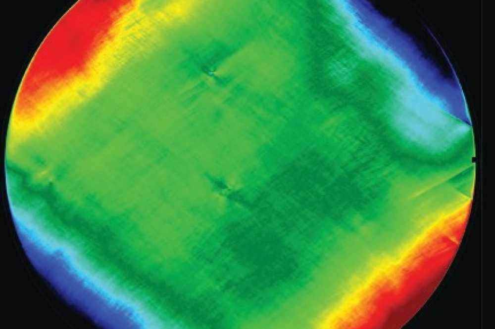
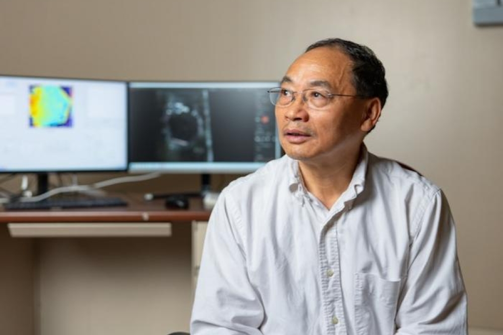
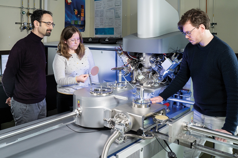
Main image: The time-of-flight secondary ion mass spectrometry tool operated by Patrik Straňák provides invaluable insights into the composition of AlYN layers, allowing analysis of interfaces and the detection of impurities.