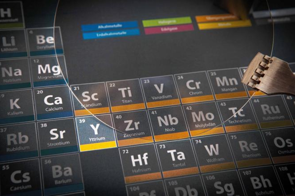
AlYN: the future for more efficient and powerful electronics?
Fraunhofer IAF researchers grow AlYN/GaN heterostructures in MOCVD reactor
The compound semiconductor aluminium yttrium nitride (AlYN) has attracted interest from many research groups, however, growing the material has been a major challenge (it could only be deposited by magnetron sputtering).
Now researchers at the Fraunhofer Institute for Applied Solid State Physics IAF have reported fabricating the new material using MOCVD technology.
“Our research represents a milestone in the development of new semiconductor structures. AlYN is a material that enables increased performance while minimising energy consumption, paving the way for innovations in electronics that our digitally connected society and its ever-increasing technology demands urgently need,” says Stefano Leone, scientist at Fraunhofer IAF in the field of epitaxy.
Recent research had already demonstrated the material properties of AlYN, such as ferroelectricity. In developing the new compound semiconductor, the researchers at Fraunhofer IAF have been focused primarily on its adaptability to GaN.
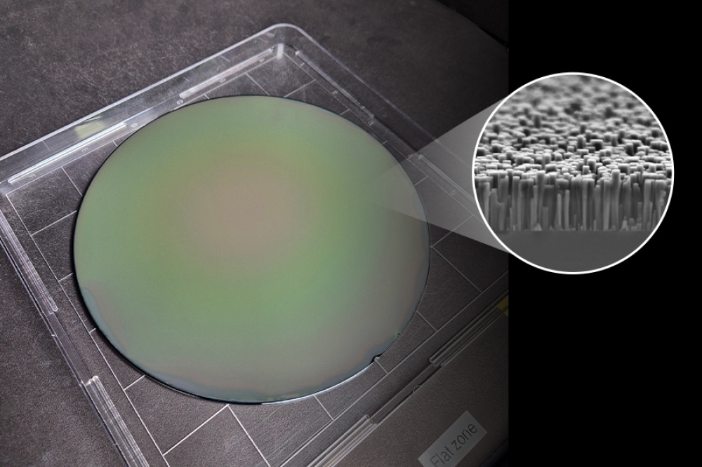
In 2023, the Fraunhofer IAF research group reported groundbreaking results when it succeeded in depositing a 600 nm thick AlYN layer for the first time. The layer with wurtzite structure contained an unprecedented yttrium concentration of more than 30 percent. Now the researchers have fabricated AlYN/GaN heterostructures with a precisely adjustable yttrium concentration, which they say are characterised by excellent structural quality and electrical properties.
The novel heterostructures have a yttrium concentration of up to 16 percent. The structural analysis group, led by Lutz Kirste, is now doing more analyses to further their understanding of the structural and chemical properties of AlYN.
The Fraunhofer researchers say they have already measured very promising electrical properties of AlYN. “We were able to observe impressive values for sheet resistance, electron density and electron mobility. These results showed us the potential of AlYN for high-frequency and high-performance electronics,” Leone reports.
The researchers observed a significant increase in electron mobility at low temperatures (more than 3000 cm2/Vs at 7 K).
The team says it has already made significant progress in demonstrating the epitaxial heterostructure required for fabrication, and continues to explore the new semiconductor for the development of HEMTs.
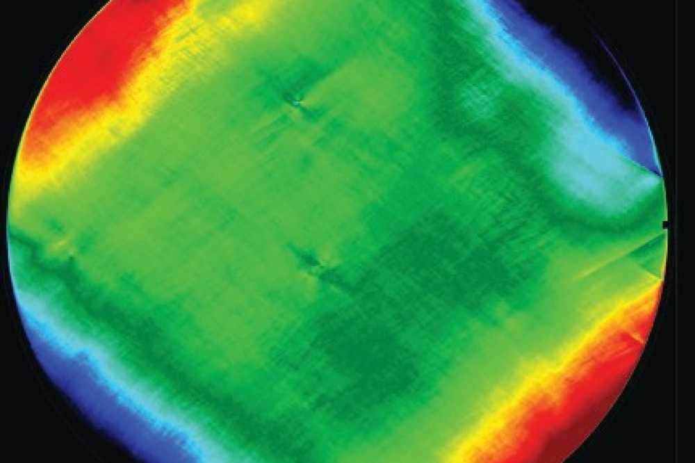
The researchers are optimistic about industrial applications. Using AlYN/GaN heterostructures grown on 4-inch SiC substrates, they have demonstrated the scalability and structural uniformity of the heterostructures.
The successful creation of AlYN layers in a commercial MOCVD reactor enables scaling up to larger substrates in larger MOCVD reactors. This method is considered the most productive for the fabrication of large-area semiconductor structures and underlines the potential of AlYN for the mass production of semiconductor devices.
A major obstacle, however, to the industrial use of AlYN is its susceptibility to oxidation, which affects its suitability for certain electronic applications. “In the future, it will be important to explore strategies to reduce or overcome oxidation. The development of high-purity precursors, the use of protective coatings, or innovative manufacturing techniques could contribute to this. The susceptibility of AlYN to oxidation is a major research challenge to ensure that research efforts are focused on areas with the greatest chance of success,” concludes Leone.
References
S. Leone et al. 'Metal-Organic Chemical Vapor Deposition of Aluminum Yttrium Nitride', Phys. Status Solidi RRL 17 2300091 (2023)
I. Streicher et al. 'Two-dimensional electron gases in AlYN/GaN heterostructures grown by metal–organic chemical vapor deposition' APL Materials 12 051109 (2024)