WHU team takes inspiration from moths to boost GaN LEDs
Researchers from Wuhan University in China have unveiled a new approach to boosting the performance of GaN-based LEDs by flexible nanoimprint lithography.
“Traditional projection lithography methods are highly sensitive to substrate shape, which can compromise the accuracy of microstructure definition on warped or irregular surfaces. Our flexible nanoimprinting technique overcomes these limitations, enabling precise and durable microstructure fabrication.” said Shengjun Zhou, a professor at Wuhan University who directed the research.
GaN-based LEDs have revolutionised the lighting industry, yet their performance has been constrained by the high threading dislocation density in heteroepitaxial films grown on sapphire substrates. Furthermore, Fresnel reflections at the epitaxial-substrate interface reduce light energy utilisation, posing additional challenges to optimising device performance.
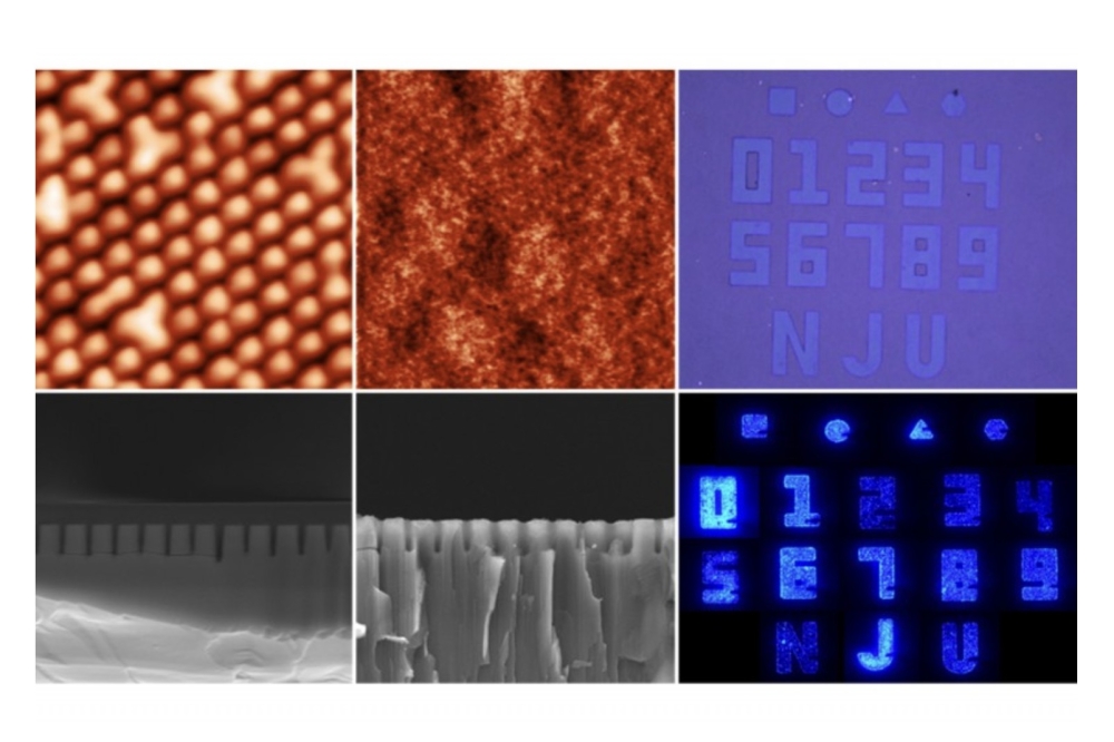
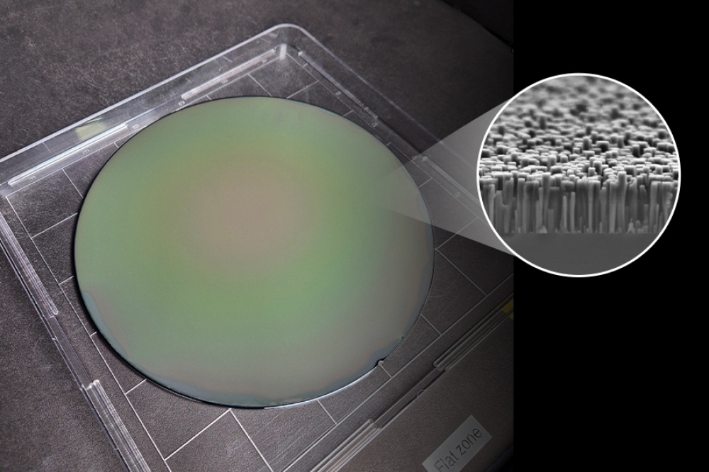
Seeking solutions in nature, the research team drew inspiration from arrays similar to moths’ compound eyes, known for their anti-reflective and light-absorptive properties. Replicating this structure in practical applications required overcoming the complexities of processing microstructures on the warped surfaces of optoelectronic devices.
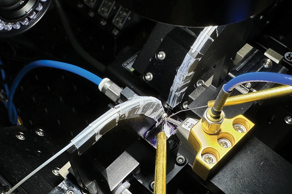
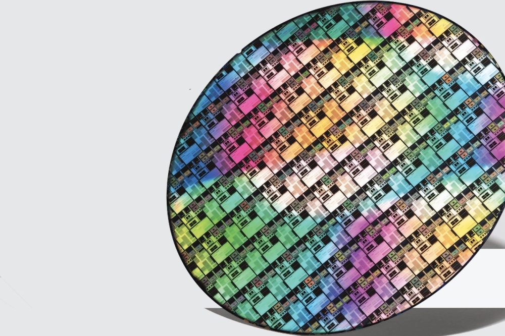
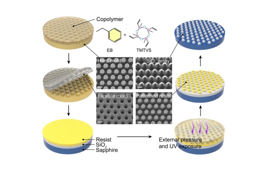
The researchers developed a flexible nanoimprint lithography process that enables high-throughput and precise fabrication of bionic microstructures on warped sapphire substrates. This process, which includes thermo-compression moulding, imprinting, UV exposure, and a uniquely designed two-step etching, resulted in the creation of a compound-eye-like silica microstructure (NCSM) template. The flexibility of this nanoimprinting method demonstrated a remarkable adaptability to substrate warpage, leading to a 6.4-fold increase in productivity and a 25 percent reduction in economic costs compared to traditional methods.
Crucially, the NCSM template significantly enhanced the performance of GaN-based LEDs. By precisely adjusting the morphology of the nucleation layer during epitaxial growth, the researchers were able to control the orientation of GaN crystal growth, achieving films with low dislocation density. Additionally, the NCSM template improved light extraction efficiency of LEDs, owing to the bionic microstructures’ photon-modulating capabilities.
As the research team continues to explore the possibilities offered by flexible nanoimprint lithography, the team says the work is poised to set new benchmarks in the miniaturisation and optimisation of GaN-based LEDs, potentially driving innovation in display technology, augmented reality (AR), virtual reality (VR), and beyond.
Reference
Flexible nanoimprint lithography enables high-throughput manufacturing of bioinspired microstructures on warped substrates for efficient III-nitride optoelectronic devices’ by Siyuan Cui, Ke Sun et al; Science Bulletin 69 (13): 2080-2088 (2024).