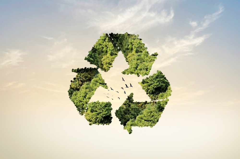
ZSW investigates perovskite PV recycling
Research scientists at the Centre for Solar Energy and Hydrogen Research Baden-Württemberg (Zentrum für Sonnenenergie- und Wasserstoff-Forschung - ZSW) in Germany are working with two industry partners to investigate how end-of-life thin-film solar modules can be reused.
The partners in the new 'PeroCycle' project want to develop an industrially viable recycling process for perovskite solar modules in four steps. Perovskite is an attractive option for the photovoltaic industry. When paired with silicon in a tandem module, the material significantly increases efficiency and can be manufactured and scaled up inexpensively.
ZSW's two partners arevSolaveni GmbH of Bönen and Solar Materials GmbH of Magdeburg. Solaveni brings expertise from the chemical processing of perovskite materials while Solar Materials specialises in the purely physical separation of composite materials without the use of chemicals.
The research scientists at the ZSW can draw on over 30 years of experience with thin-film solar modules and over ten years of materials research on perovskite solar cells and modules. The German Federal Environmental Foundation (Deutsche Bundesstiftung Umwelt - DBU) is funding the joint project.
Making perovskite modules recyclable
The aim of the research team is to develop an industrial recycling process to enable the optimum reutilisation of end-of-life modules.
The first step to this end is the manufacture and encapsulation of perovskite mini-modules at the ZSW. “Given the sharp increase in the number of PV module installations, there is always a need to consider the issue of recycling, and this must be done at an early stage in case of new technologies like perovskite solar modules,” said ZSW employee Cordula Wessendorf, talking about the PeroCycle project.
The second step calls for the use of thermomechanical processes at Solar Materials for the separation of the encapsulated perovskite modules. This involves testing whether the glass-polymer composite and therefore the glass as a whole can be effectively separated from the perovskite absorber material. Unlike conventional shredding processes, there is no mixing with other materials in this case. The glass can therefore be processed into container glass. The perovskite absorber material is collected separately.
Step three follows the separation of the materials and entails the development and optimisation of a perovskite recycling process at Solaveni. Non-flammable, cost-effective and environmentally-friendly solvent systems have been developed specifically for the recycling process, obviating the need for toxic solvents and avoiding the deployment of extreme conditions, such as high temperatures.
The new approach reduces energy consumption and waste, making it possible to cut costs and minimise environmental impact. The future recycling method includes chemical and physical processing techniques. The aim is to recover at least 90 per cent of the perovskite with a purity of 99 per cent.
The fourth and final step will be to make a new perovskite module at the ZSW from the materials obtained. The recycled perovskite absorber material and the recycled glass coated with transparent contacts will be used for this purpose. The research scientists in the materials laboratory aim to achieve at least 90 per cent of the efficiency of the freshly produced reference samples from the recycled materials.
The ZSW will be presenting the latest developments in PV recycling at the PV recycling workshop on 14 and 15 October 2024 in Stuttgart.