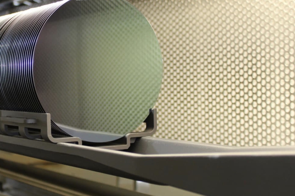
SICC shows first 300mm SiC wafer
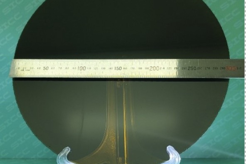
At Electronica 2024, Chinese SiC wafer company SICC will exhibit what is thought be the first 300mm N-type SiC substrate.
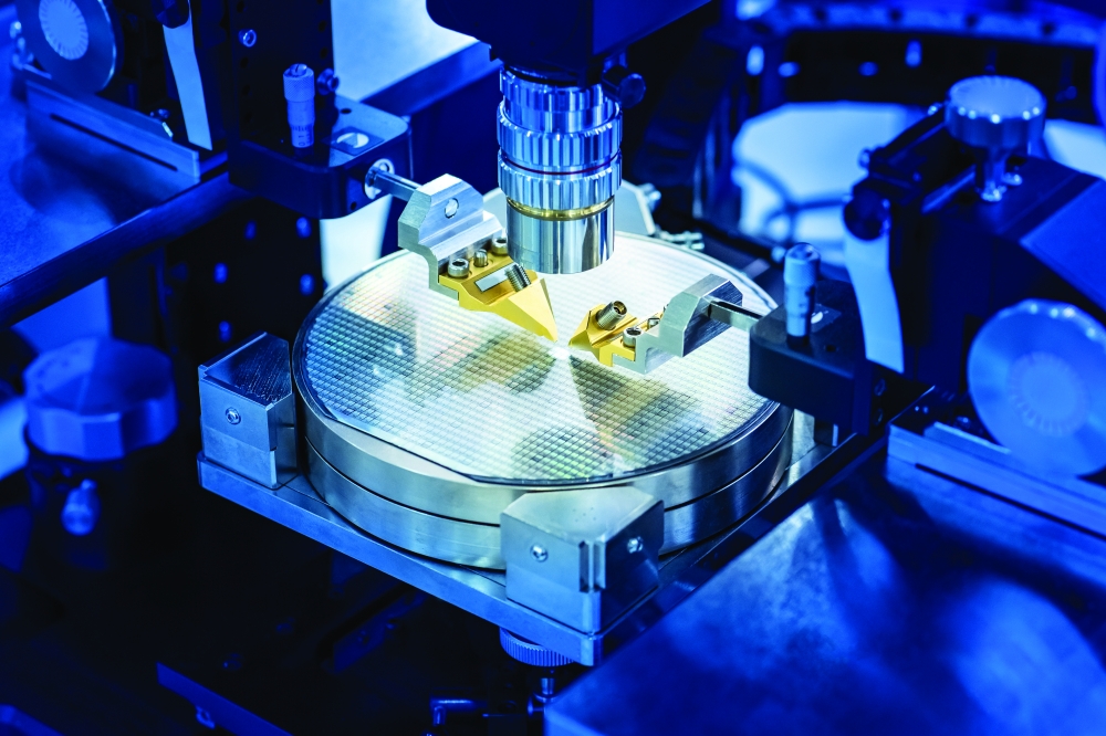
SICC already makes 150mm and 200mm N-type conductive SiC, and high-purity semi-insulating substrates. The company has also developed large-size P-type SiC substrates.
But the 300mm N-type substrate, it says, is an industry breakthrough that highlights SICC's ability to push the boundaries of semiconductor technology.
For example, in its 200mm conductive 4H-SiC single crystal substrates, SICC says it has achieved near-zero threading screw dislocation (TSD) and extremely low basal plane dislocation (BPD) densities, which significantly enhances yields.
For its high-purity semi-insulating SiC substrates, SICC claims zero micro pipe density. (Micro pipes are SiC crystal defects that can cause electronic devices to short circuit and fail).
The company puts this success down to the ability to precisely control the crystal growth process, ensuring consistent wafer quality .
The company, which has headquarters in Jinan, is currently further expanding its 200mm SiC wafer manufacturing capacity at its Shanghai plant.