Enhancing β-Ga₂O₃ with hetero-integration
Thanks to the introduction of a far higher thermal conductivity and p-type doping, better devices are realised when pairing β-Ga2O3 with SiC or diamond.
BY ARPIT NANDI, ADITYA BHAT, INDRANEEL SANYAL, SAI CHARAN VANJARI, JAMES
POMEROY, MATTHEW SMITH AND MARTIN KUBALL FROM THE UNIVERSITY OF BRISTOL
Climate change and unpredictible extreme weather are impacting human life more frequently than ever. In just the last few months many in central Europe have suffered from such events, with severe flooding occuring at the same time that more than 5,000 firefighters were fighting wildfires in northern Portugal. These events underscore the urgent need to decarbonise the energy sector, an endeavour where power electronics can play a crucial role.
Within the power electronics portfolio, different materials are seeing deployment at different voltages. For low-to-medium-voltage applications, it is the silicon-based devices that dominate, due to their cost-effective manufacturing processes. But in the mid-to-higher voltage range, GaN and SiC have gained traction, with GaN-on-silicon benefiting from silicon-style manufacturing. And there is also Ga2O3 to consider – it has emerged as a highly promising material for power electronic devices, due to its large bandgap (4.8 eV), its tolerance for high electric fields (8 MV cm-1), and the promise of cheaper production than the more established SiC.
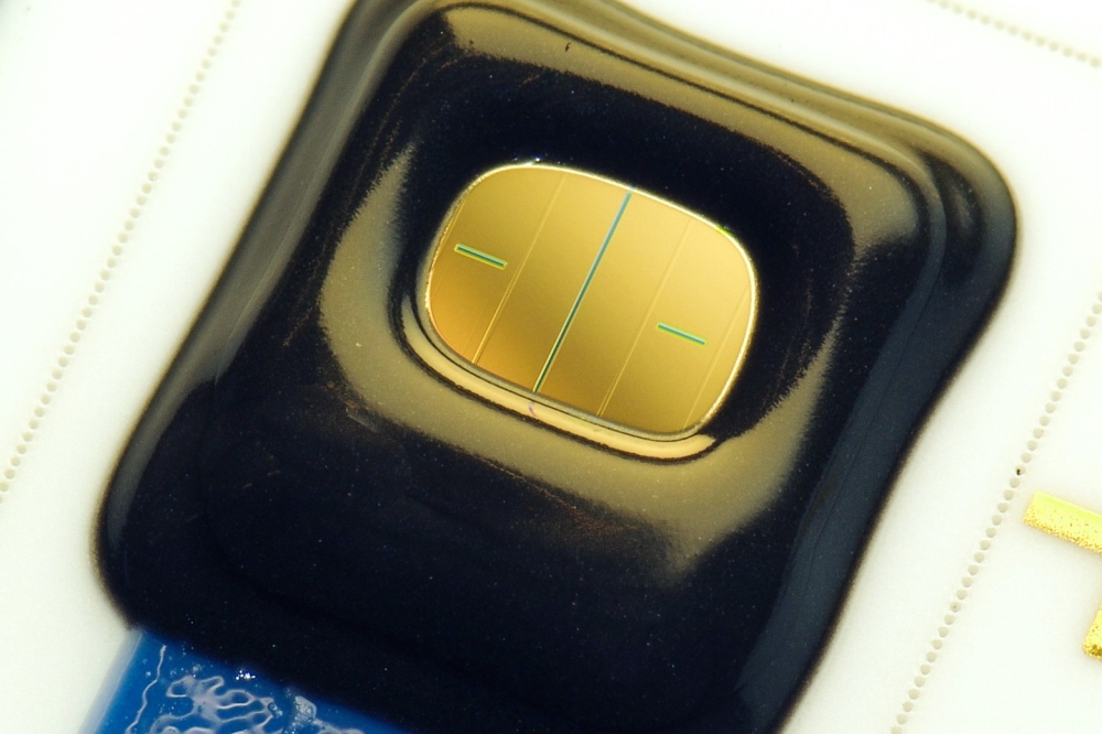
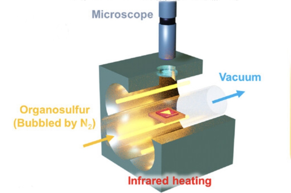
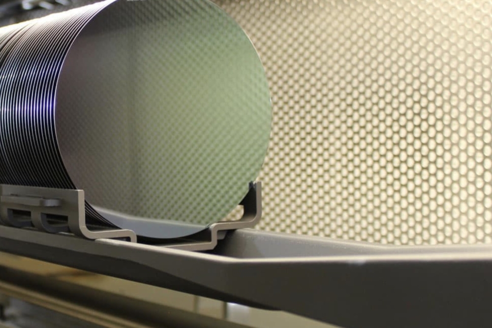
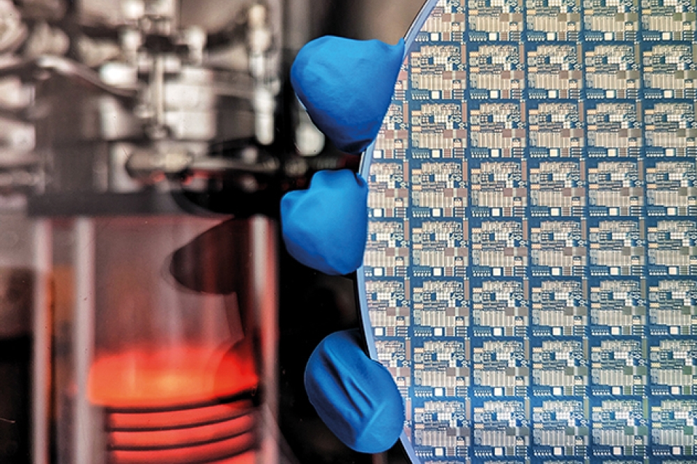
Figure 1.(a) and (b) Ga2O3 MOCVD, and (c) clean room facility at the University of Bristol.
Researchers working with this ultra-wide bandgap oxide have enjoyed tremendous success over the last decade or so, with interest ignited by the first report of a Schottky barrier diode in 2013. Spurred on by this triumph, alongside the ease of n-type doping and the availability of melt-grown substrates, these pioneers are now gaining further encouragement as 6-inch substrates appear on the horizon, as well as a push from multiple material vendors across the globe. There are now producers of Ga2O3 substrates in Japan, the US, Germany, South Korea and China. Based on all this promise, commercialisation of Ga2O3 looks inevitable for high-voltage applications.
Those developing Ga2O3 material and devices include the UK government-funded Innovation and Knowledge Centre REWIRE, led by our team at the University of Bristol. While we acknowledge that today’s Ga2O3 devices exhibit excellent performance, with breakdown voltages that can exceed 8 kV, there are drawbacks that we are starting to address. Significant concerns preventing this material from harnessing its full potential include an on-state currents that’s relatively low, and a device reliability that still needs to be established and proven.
Figure 2. (a) Cross-sectional TEM image, low magnification plan view of
Ga2O3 thin film grown on diamond. (b) The rocking curve illustrates
grain size increase after incorporating an improvised seeding layer,
reflecting a decrease in FWHM.
Behind these limitations are: a lack of useable p-type doping for Ga2O3, primarily due to the flatness of the valence bands; and a low thermal conductivity. But there are ways to mitigate this through the heterogeneous integration of Ga2O3 with SiC and diamond – they are materials with high thermal conductivity and p-type doping. Combining Ga2O3 with other materials is an increasingly popular approach to tackling the critical technological bottlenecks. For example, Ga2O3 MOSFETs attached to diamond through mechanical exfoliation and bonding are showing good promise, as are devices featuring composite wafer fabrication with SiC. Still, concerns remain related to scalability, impairing manufacturing. Note that in addition to Ga2O3 and its alloys, REWIRE is exploring, amongst others, SiC, AlGaN, diamond and BN device technologies, in a team with partners at Warwick University and Cambridge University.
Powered by state-of-the-art growth and clean room facilities at the University of Bristol, we are approaching heterogeneous integration of Ga2O3 in various ways. Our goals include: optimising Ga2O3 heteroepitaxy on SiC and diamond substrates, the latter in collaboration with Element Six Technologies and Orbray; and in partnership with Srabanti Chowdhury’s Wide Bandgap Lab at Stanford University, exploring thin p-type diamond overgrowth on Ga2O3.
Pairing Ga2O3 with diamond…
Pairing Ga2O3 with diamond is very attractive. With a bandgap of 5.4 eV, p-type conductivity, a thermal conductivity of up to 2000 W m-1 K-1, and a predicted critical electric field strength of 10 MV cm-1 – that’s even higher than that of Ga2O3 –diamond compliments and enhances the effectiveness of Ga2O3 when its adequately integrated.
Our initial work on this front has involved the growth of Ga2O3 on single-crystalline diamond substrates. For this effort, we faced two underlying challenges: prevention of oxidation of the diamond surface at high temperatures during initial growth stages; and overcoming the challenge of realising good nucleation, which is plagued by the high surface energy differences between Ga2O3 and diamond.
To address these concerns, we have pursued a two-step process, beginning with the low-temperature growth of a thin layer of Ga2O3 that protects the diamond surface, followed by high-temperature growth of an epitaxial layer. Our detailed analysis of the microstructures and grains produced during this process has revealed two-grain variants aligned to [110] diamond and its perpendicular direction. Due to a peculiar asymmetric hexagonal (-201) face and mirror symmetry, each set has its own four equivalent subvariants (for more details see Nandi et al. Crystal Growth & Design 23 8290 (2023)).
Figure 3. (a) 3-D visualization of simulated Ga2O3 / diamond
superjunction diode, (b) schematic of planar p-n diode fabricated and
(c) its measured reverse breakdown at –875 V.
One of the important outcomes of our study is that it has helped us to identify the off-cut directions that are needed to eliminate grain variants and improve the epitaxial structure. Our approach is following in the footsteps of many other prior material systems, given that the use of off-cut substrates has a strong and well-established track record in reducing the multiplicity of grain variants. We have employed Ga2O3 growth on off-cut diamond substrates to refine the quality of the epitaxial layers and eliminate one set of sub-grains. By introducing a unique, improvised seeding layer, we have produced better, smoother coalesced surfaces with larger grains and similar sets. With this approach we have grown a variety of layers, including that with a thickness of around 250 nm (see Figure 2 (a)).
Another part of this work has been the growth of an n-type doped Ga2O3 cap layer on undoped material. This epistructure is a starting point for fabricating quasi-vertical power devices, currently under development. Supporting such efforts is the availability of 2-inch free-standing diamond substrates, with p-doping of this material set to follow.
…and SiC
Composite bonded SiC-Ga2O3 substrates have also been gathering interest, due to their potential to deliver a significant reduction in the Ga2O3 device temperature. However, the weak van-der Waals bonding at the interface between the two materials threatens to impede the mass adoption of such an approach, effectively impacting yield.
One alternative is the heteroepitaxy of Ga2O3 on SiC; though similar to growth on both sapphire and diamond, this is a rather complex process with limited thermodynamic understanding. To try and shed new light on this, we have established a detailed thermodynamic picture that encapsulates the growth of Ga2O3 on foreign substrates, and assumes a Volmer−Weber growth mode, where the substrate surface energy is lower than the epilayer surface energy.
Our investigations have determined that growth of Ga2O3 on SiC is favourable at higher temperatures, a finding that falls in line with the widely adopted approach for growth on sapphire substrates. A preference for higher temperatures on both these foundations is mainly due to the comparable interface energies required for forming Ga2O3 islands during nucleation with unit volume.
Figure 4. (a) Schematic of trench Schottky barrier diode fabricated at
the University of Bristol and its (b) forwards and (c) reverse
characteristics.
Heterogeneous device engineering
In addition to materials integration via growth, improved device engineering is critical to alleviating Ga2O3 challenges. Diamond promises to play a role, thanks to its capability to combine excellent heat extraction with p-type conduction, realised by boron doping. This conductivity opens the door to advanced device architectures that combine a low conduction loss with a high breakdown – a combination that can break through the typical trade-off between on-resistance and breakdown.
A team from Xidian University have pursued this type of approach, uniting p-type NiO with n-type Ga2O3. Devices with a breakdown voltage of more than 8 kV have followed, an outstanding result. However, the practical potential of these devices may be limited by the low thermal conductivity of both constituent materials, a weakness that ultimately restricts the current-carrying capacity.
Promising to overcome this limitation is the super-heterojunction Schottky diode formed from n-type Ga2O3 and p-type diamond (Figure 3 (a)). Simulations suggest that this device, which we are pursuing, can deliver off-state breakdown voltages of more than 4 kV, and an on-state resistance of just 2-3 mΩ cm2. The introduction of diamond quashes the peak temperature rise by up to around 60 percent compared with conventional Schottky diodes; and the advanced device structure aids electric field management in Ga2O3. We expect this super-heterojunction diode to drastically outperform SiC in medium and high-voltage DC power converter applications where there is a low elevation in case temperature.
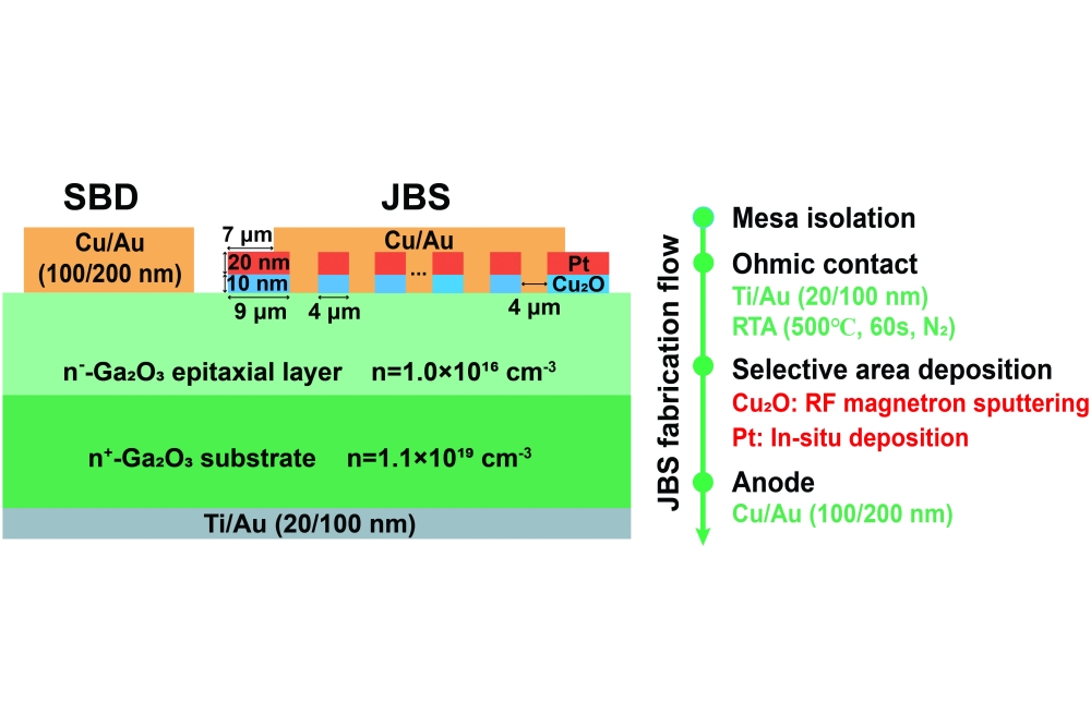
The working principle of the super-heterojunction Schottky diode that pairs n-type Ga2O3 and p-type diamond builds on the prior three-dimensional Ga2O3 device structures of trench Schottky barrier diodes. It is well known that despite the high critical electric field strength of Ga2O3, devices based on this oxide are yet to deliver a high breakdown, due to catastrophic breakdown that stems from a peak electric field at the metal-Ga2O3 interface in planar Schottky diodes. This peak field is behind the early breakdown and unreliable device operation. Trench Schottky barrier diodes offer some promise in this regard, as they have been shown to push the peak electric field away from the interface and reduce the surface electric field (see Figure 4). We are not alone in demonstrating devices that operate on this principle – other groups have also enjoyed success, such as teams from Cornell University and the University of California, Santa Barbara.
By reducing the surface electric field, due to sidewall MOS capacitances, we have trimmed the parasitic leakage current and realised an off-state breakdown of more than 3 kV (see Figure 4 (c)). Previously we reported that fins fabricated along [010] orientation deliver the highest current and the lowest parasitic charge trapping. In sharp contrast, fins with the [100] orientation show poor reliability. Another interesting finding by our team is that according to UV-assisted capacitance measurements, Al2O3 dielectrics for MOS capacitors show less trapping, suggesting that they could ensure a more reliable device performance. We are in the process of assessing failure modes and reliability of Ga2O3 trench Schottky barrier diodes.
Combining knowledge from device simulation and fabrication, we have taken the first steps towards realising super-heterojunction diodes based on p-type diamond and n-type Ga2O3. These efforts began by optimising and characterising the interfaces between these two materials, with studies investigating 100 nm-thick boron-doped diamond, grown on n-type Ga2O3 that has been deposited at Stanford University using the microwave plasma CVD technique.
Electrical measurements of devices we’ve made in this manner have produced promising results, including a catastrophic breakdown of 875 V with a peak electrical field of 4 MV cm-1, which could be reduced with appropriate edge-termination techniques. Based on these results, integrating these materials in the three-dimensional structure that’s illustrated in Figure 3 (a) would enable a breakdown voltage of more than 4 kV in that super-heterojunction device. The planar diode also exhibits a low thermal resistance, confirming that diamond delivers excellent heat extraction when deployed in advanced device structures based on Ga2O3. Additional promising findings, emerging from Chowdhury’s group at Stanford University, are diamond integration using low-temperature CVD, and demonstrating the possibility of the same on Ga2O3.
There’s no doubt that Ga2O3 possesses impressive material properties that ensure it will play a vital role in the power electronics sector. To enhance such success, this oxide should be integrated with other ultra-wide bandgap materials, such as diamond and SiC, that can improve electro-thermal co-design. Note also that Ga2O3 has several polytypes, and while we have focused on the βform, other phases should not be forgotten – they provide an opportunity to explore even higher bandgaps and also polarisation. Like other research groups, we are exploring these forms.
Such efforts will help to advance the capabilities of Ga2O3 devices, which we forecast to provide a prolonged device lifetime, along with gains at the system level, in terms of size, weight and efficiency. Early studies of converters that employ Ga2O3 are already demonstrating potential system benefits, which can lead to a trimming of carbon footprints and help to turn the tide on an escalation in the frequency and severity of natural disasters.


