Progress opens the door to viable quantum markets

Recent successes in the scale-up of quantum photonic components is giving the green light to system-level product manufacturers looking to capitalise on Quantum 2.0 effects.
BY DENISE POWELL AND WYN MEREDITH FROM THE COMPOUND SEMICONDUCTOR CENTRE
While interest in quantum technologies is eclipsed by that in AI, it is still grabbing a great deal of attention. And that’s not surprising, given that this sector is forecast for tens and even hundreds of billions of dollars per annum over the coming years.
Such figures are attracting individuals and companies with an entrepreneurial spirit to consider pursuing opportunities in quantum markets. That includes system integrators, looking to leapfrog from successful demonstrators to commercial quantum products.
Unfortunately, it’s not easy for system integrators to succeed in this endeavour. As well as having to overcome the significant technical difficulty of realising robust quantum systems, their progress has been held back by two critical obstacles. The first of these is having access to a wide pool of end-users willing to commit time and resources to evaluating systems and creating use cases. And the second, more fundamental obstacle to the viability of quantum markets, is that unless quantum laser sources and detectors are readily available at sufficient yields – and thus acceptable price-points – quantum technologies will always be limited to high-margin and low-volume mission-critical applications.
Illustration of an ideal, under-control 6σ process that operates within the product specification limits.
Here we will focus on the latter issue. When tackling this, it’s important to note that the specifications governing quantum photonic components (QPCs) are so tough to fulfil that unviable processes will prevent component prices from falling to acceptable levels, thereby creating a barrier for volume markets to emerge. Quantum markets are not immune to the basic principles of supply and demand, and end-users must evaluate where the quantum advantage delivers a justifiable benefit within their product offerings.
While this outlook is not what many wish to hear, it is not merely pessimism, but reflects manufacturing process controls. In a well-controlled environment that is adhering to a 6σ methodology, control limits encompass the process distribution, while the specifications relating to the product are wider, to ensure zero defects.
During the manufacture of many forms of compound semiconductor devices, it’s not unusual for them to fall outside the 6σ standard. However, when that happens, product specifications governing industrial processes tend to generate budget yields that are still sufficiently viable for market adoption. For QPCs, however, the situation is starkly different, with product specifications only encompassing a small proportion of standard manufacturing process capabilities.
So what does this mean? Let’s consider the VCSEL, a class of laser that’s employed to pump and probe transition lines of atomic species when it is serving in quantum applications. The typical uniformity of epiwafers used for high-volume VCSEL products, such as for sensing applications, is too non-uniform for quantum applications. An epiwafer controlled to the same uniformity distribution would only provide a narrow ring that is suitable for QPC device fabrication, if we assume that the wafer’s uniformity has a radial profile. Making matters even more challenging, there’s a need to meet tight specifications at the device level on parameters such as power and single-mode operation. Given all this, we can expect that commercially viable yields for QPCs will be extremely low. While it is possible to produce thousands of die on a single 100 mm wafer, an incredibly small proportion of these lasers are going to be single-mode, polarisation-stable VCSELs that combine the right output power with acceptable values for threshold current, temperature and current-tuning coefficients, and also fall inside the stringent operating temperature window while emitting a near-perfect beam profile.
Is it unreasonable to pick the VCSEL in this discussion of QPCs? Certainly not, given that VCSEL fabrication is a relatively mature process. Difficulties arise because it is challenging to scale device production for quantum applications, due to the stringent specifications required, as well as the need for single-mode performance.
Illustration of typical relationship between the overall manufacturing
process distribution to the lower and upper product specification limits
(LSLQT and USLQT) for quantum applications.
To help address this challenge, since September 2020 our team at the Compound Semiconductor Centre has led a project involving twelve partners across the UK aimed at improving the manufacturability of QPCs. However, the ultimate goal of this £5.8 million three-year programme, which is known as QFoundry and is part-funded by the UK Quantum Technologies Challenge, under UK Research & Innovation, is the establishment of robust and resilient supply chains that are committed for the long-run.
The QFoundry project has focused on the viability of QPCs that are urgently needed for the commercialisation of demonstrator systems in atomic clocks, quantum magnetometers, gyroscopes, lidar and quantum key distribution. These applications are viewed as relatively mature at the systems-level compared to quantum computing, suggesting market adoption will be earlier. This expectation is in-line with a number of publicly available roadmaps, including the Optica Quantum Photonics Roadmap: Every Photon Counts, released in 2020. Supporting this prediction are reports arguing that quantum computing business models are more likely to be based on high-value/low-volume, shared-access hardware, while sensing and quantum key distribution applications will drive relatively higher volumes at the QPC-level – making the latter a more attractive business proposition for compound semiconductor supply chains.
Status quo for semiconductors
Scale-up is, undoubtedly, the latest buzz phrase to hit the quantum scene. For industrial semiconductor supply chains, however, this task is their bread and butter; each new technology platform has to undergo extensive scale-up activity to understand and address critical process interactions, establish control limits and ensure inherent manufacturing repeatability, reproducibility and reliability. These principles have underpinned the QFoundry approach to deliver notable progress across VCSELs, quantum dots and single-photon avalanche diodes (SPADs).
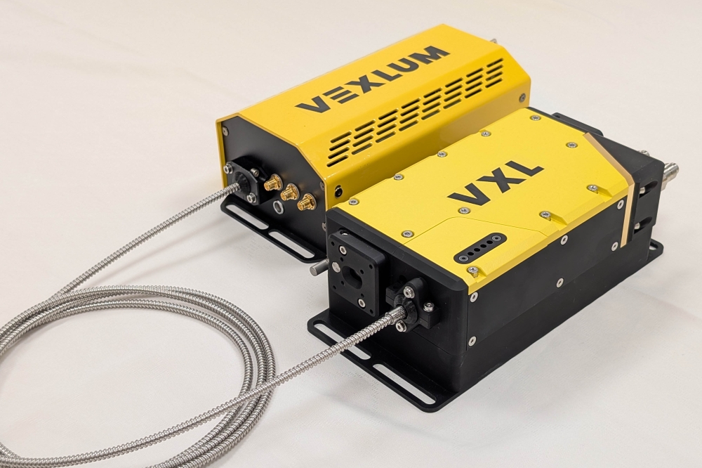
Following three years of activity, the UK supply chain is now offering the world’s broadest portfolio of single-mode VCSELs tailored to quantum applications, with lasers spanning 760 nm to 940 nm. Encouragingly, these VCSELs are manufactured with a threefold improvement in yield at the device level as a result of efforts to drive semiconductor material uniformity at CSC, and major advances in device design, chip fabrication and characterisation by the team at Integrated Compound Semiconductors.
What is particularly pleasing is a reduction of almost 60 percent in the R&D effort and cost required to develop a new device against custom specifications, thanks to improvements to the models that are designed to closely match manufacturing processes. These models have been refined through iterative development, enabled by QFoundry. Another triumph is that these devices have realised more than 10 years of operation at 70 °C under accelerated ageing conditions, demonstrating that they can serve in atomic clocks deployed in low earth orbit applications. To increase their capability for these missions, we plan to carry out additional device reliability testing.
QFoundry has derived much benefit from its technology validation partners, such as Toshiba and the National Physical Laboratory (NPL). These collaborators have expertise in validating QPCs in custom, application-relevant testbeds.
Our efforts have re-enforced our view that quantum technology development desperately needs supply chain partners that translate application requirements through to appropriate component specifications. Progress on this front has been a big factor in the success of QFoundry.
One example, highlighting this point, is the identification of system-level noise caused by standard TO-can packaging. The team at NPL are leading experts on atomic clocks and were able to identify the problem and work closely with Bay Photonics on re-designs and custom package development. Following successful demonstration, those at Bay have invested in the automation of VCSEL packaging, and are now ready to support the quantum community with volume ramp.
For quantum dots and SPADs, the challenges are starkly different to those faced for the VCSEL, despite also using iterative development for material and process improvements. This discrepancy is due to decades of industrial research in the epitaxial structures and fabrication of the VCSEL, which has propelled this device to a technology readiness level that is well ahead of that for quantum dots and SPADs. Much effort has been devoted to materials development, to address the background emission of quantum dots and the dark currents of SPADs. Progress has also required a lot of manpower to ensure that the fabrication processes lead to robust device operation.
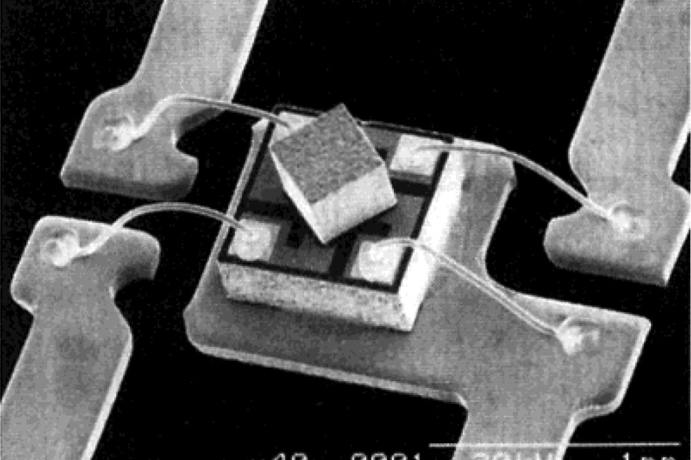
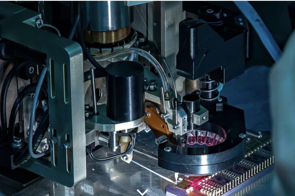
Automated die bonding at Bay Photonics of customised TO-can packages for atomic clock applications.
Despite these challenges, the QFoundry quantum dot and SPAD partners have made significant progress. Milestones for quantum-dot development include the development of reproducible droplet epitaxy on an industrial MOCVD reactor, as well as: forming structures that produce a low-background emission from different growth methods, the realisation of functional fabrication processes, and recording long coherence times at telecom wavelengths.
Our SPAD development has benefited from previous prototyping. Drawing on this expertise, partners in the QFoundry partners have scaled-up epitaxial growth from 50 mm to 75 mm wafers with processes that allows the detector’s temperature to be managed with thermo-electric cooling, thanks to extensive custom butterfly package development at Bay Photonics.
The advances that we have made, in terms of the technology readiness level, are giving confidence to quantum system communities. While challenges remain, we are seeing a viable pathway to robust supply of quantum photonic components. The next step is for the quantum community to work hand-in-hand with the compound semiconductor supply chain to ensure that system-level development does not run away with specifications that further constrain the viability of quantum technologies.
Is it really worth it?
Many may question whether the gruelling efforts across the QFoundry partners make sense, given that quantum markets are yet to be established. But there are times when supply chains must take the long-term view and co-invest in technologies, even though entry into mainstream markets is a question of when, rather than if. The quantum industry is in a situation that can be likened to a Mexican standoff, where someone has to pull the trigger first. It is only when supply chains are robust and validated that system integrators can commit to offering quantum systems. In this case, QFoundry partners have dived headfirst, but they are reaping rewards that are far greater than ever anticipated.
Quantum is perhaps one of the few mystifying areas of research, where the sum of the parts is definitely bigger than the whole, as well as the whole being bigger than sum of the parts. Developments across each step of the supply chain have yielded incredible insights and capabilities that would have never come during more typical laser and detector development. We have uncovered subtle, yet critical interdependencies and process interactions that govern QPCs that sit deeply within the relatively slack tolerances associated with standard, non-quantum applications.
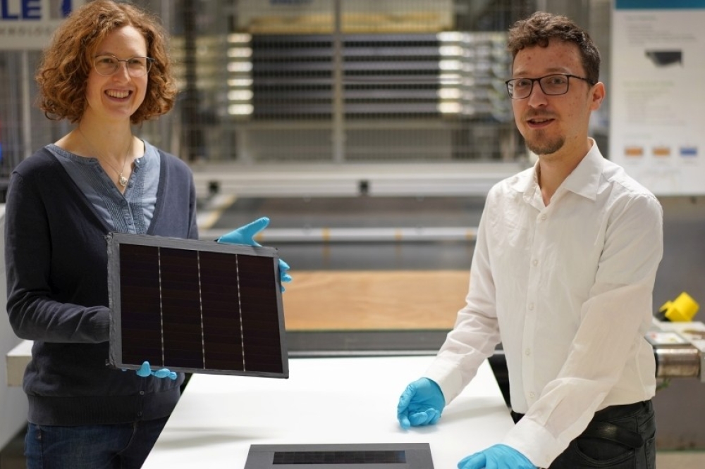
Successful scale-up of SPAD fabrication from 50 mm to 75 mm substrates at the University of Cambridge.
Those of you that have had the pleasure of visiting high-tech research facilities, such as the UK’s Harwell Campus, will appreciate the enormity of the capability that must be developed in order to address unknown unknowns that arise. What can initially appear as a distraction often leads to insights and know-how that can be rewarding beyond the original scope and goals of a technical challenge.
Ultimately, a significant amount of expertise and intellectual property has been developed across the QFoundry partner base, with the project establishing robust supply chains that do not shy away from hard-to-hit specifications. On the other hand, semiconductor foundries serve markets best when specifications converge, which is equally relevant to quantum systems.
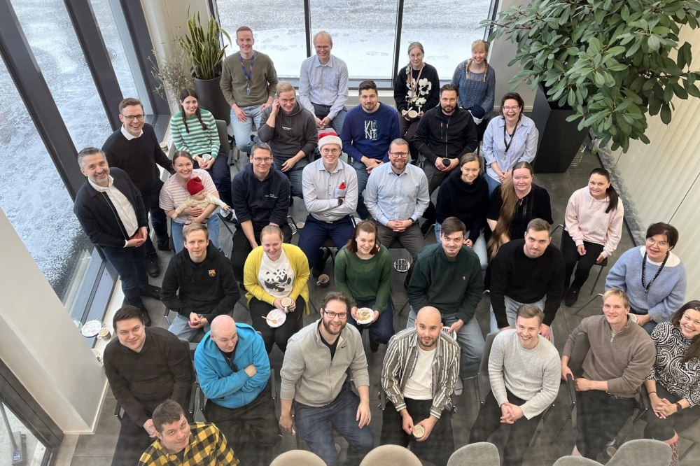
The 12 partners in the QFoundry project.
One of the legacies of QFoundry is that it has set the scene for an industrial approach to addressing the viability of quantum markets. Timing is everything and having established baseline process windows, all the partners in QFoundry are ready to work with the quantum community in developing custom QPCs across different verticals. The work is never complete in the semiconductor industry; product launches are followed by intensive continuous improvement, and quantum technologies are at the very beginning of their journeys. But one thing is certain: there is no world of quantum without compound semiconductors.

