Advancing GaN power devices with ammonia MBE
Operating in the kilovolt regime, GaN vertical p-n high-power diodes
produced by ammonia MBE combine a fast growth rate with an ultra-clean
thick drift layer and a smooth surface morphology.
BY ESMAT
FARZANA,* JIANFENG WANG, KAI SHEK QWAH, ASHLEY WISSEL-GARCIA, KELSEY
JORGENSEN, TAKEKI ITOH, ZACHARY BIEGLER, MORTEZA MONAVARIAN AND JAMES
SPECK FROM THE UNIVERSITY OF CALIFORNIA, SANTA BARBARA
THE LAST FEW YEARS have seen a surge in demand for efficient power devices. It’s a ramp that’s been spurred on by the rise of a number of next-generation technologies, including fast chargers, data centres, smart grids, high-speed telecommunication, and electric transportation.
For these high-power switching applications, today’s silicon-based technology is not up to the task, with concerns surrounding its poor efficiency, excessive voltage levels, bulky system volume, extensive heating, and power loss. This has driven interest in alternatives based on newer materials systems, such as wide bandgap semiconductors, which are attracting much attention thanks to their capability to enhance power-handling while shrinking system size. Amongst these promising candidates GaN has much appeal, thanks to its excellent combination of a high material breakdown field of around 3.3 MV cm-1, a high mobility, good thermal conductivity, and the availability of both p-type and n-type material.
With such attractive properties, it’s of little surprise that GaN has already been adopted in a wide variety of commercial electronics, including RF transistors, power amplifiers, and LEDs. However, for the case of power electronics, commercial GaN devices tend to be limited to 650 V, typically employing lateral topologies.
Switching to a vertical device geometry enables an increase in the operating range beyond 650 V, thanks to a superior electric field confinement and enhanced current capability, supported by a large-area backside contact. However, to enter the multi-kilovolt range, these vertical power devices need to have thick GaN drift layers with very low and well-controlled doping alongside minimal compensation.
Historically, it has been difficult to address these challenges, due to a lack of freestanding high-quality native substrates. This limitation explains why much of the development of conventional GaN devices has taken place on foreign substrates, such as sapphire and silicon. One downside of these heteroepitaxial growth platforms is that they lead to a high dislocation-density in the epilayers – it is about 108 cm-2. Such a high dislocation density may still be tolerable in lateral RF transistors, because dislocations remain perpendicular to the lateral channel. However, that’s not the case in vertical devices, where the threading dislocation core directly appears along the vertical channel. For these devices, dislocations severely degrade device performance, creating a high leakage, reducing breakdown voltage, and impairing current transport.
Figure 1. Unintentional background doping in ammonia MBE GaN epilayers
as a function of growth rate. The GaN-on-GaN epilayers provided the
lowest doping compared with the GaN-on-sapphire ones. For more details,
see APL Materials 9 081118 (2021).
In recent years this state-of-affairs has shifted, due to rapid advances in freestanding GaN substrates, which have significantly lower dislocation densities, ranging from 104 cm-2 to 106 cm-2. These far lower dislocation densities are opening new doors and starting to redefine the landscape of GaN power devices. Within the GaN community, efforts are now being directed at the development of efficient strategies for growing thick epitaxial layers with low impurities that will ensure the desired high-voltage rating with vertical device structures. However, growing thick epilayers is challenging. It demands fast growth rates, comparable or more than 1 µm hr-1, to ensure timely growth, a requirement that leads to increases in impurity concentration and surface roughness.
A significant research effort over many years has involved improving the quality of thick GaN epilayers on native substrates. However, these reports tend to focus on MOCVD-growth of GaN. It’s an epitaxial technology that offers a fast growth rate, but due to the use of a chemical-vapour-based synthesis process involving precursors, such as trimethylgallium, it often introduces a high concentration of carbon and hydrogen impurities in the GaN epilayer. These impurities are a menace, dragging down doping efficiency in GaN, due to a combination of donor compensation effects by carbon, and magnesium acceptor passivation effects by hydrogen. Due to these issues, it is far from easy to realise controllable doping over a wide range in n-type and p-type GaN with conventional MOCVD.
Figure 2. Atomic force microscopy scans of 2 µm by 2 µm area for
unintentionally doped ammonia MBE GaN epilayers (a) on GaN-on-sapphire
template using an indium flux beam-equivalent pressures of 0 Torr (b) on
GaN-on-sapphire template using an indium flux 5 × 10⁻⁸ Torr (c) on a
Mitsubishi Chemical Corporation free-standing GaN substrate using indium
flux beam-equivalent pressures of 5 × 10⁻⁸ Torr. Homoepitaxial GaN
growth on a free-standing GaN substrate shows the smoothest surface
morphology with very low root-mean-square roughness of 0.21 nm. For more
details, see APL Materials 10 081107 (2022).
Ammonia MBE for thick GaN
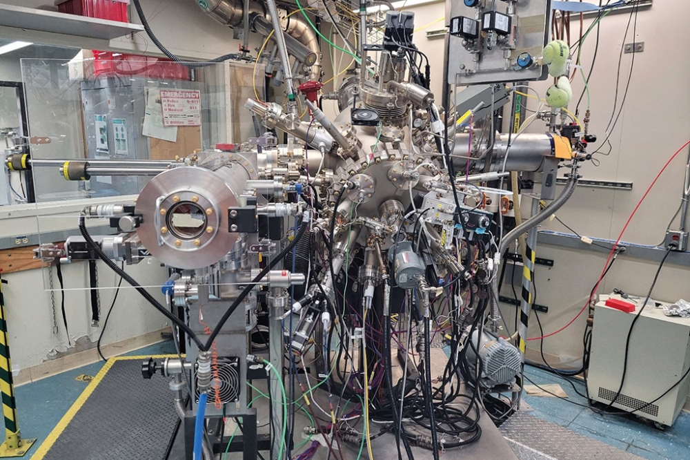
To overcome these challenges, our team that is based at the University of California, Santa Barabara (note that some of us have recently moved on, taking up academic positions elsewhere) have developed an alternative approach to growing thick GaN epilayers that employs ammonia MBE.
Compared with MOCVD, all forms of MBE offer four key advantages: a clean growth environment in an ultra-high vacuum, which allows the formation of high-purity GaN layers with a background doping as low as 1015 cm-3, as well as minimal compensating impurities, such as carbon and hydrogen; a controlled doping profile over a wide range of concentrations, spanning the mid 1015 cm-3 to 1020 cm-3, thanks to minimal compensating impurities; fully activated as-grown p-GaN, due to an absence of hydrogen passivation effects; and the opportunity to form an abrupt p+-n junction, due to absence of the magnesium memory effect, a well-known challenge in MOCVD GaN growth.
Within the family of MBE, ammonia MBE offers additional advantages over its plasma-enhanced MBE counterpart. The latter utilises gallium-rich growth conditions, while ammonia MBE allows the growth of GaN deep within the nitrogen-rich region. Due to this, ammonia MBE eliminates gallium droplets, a problem that plagues plasma-enhanced MBE and causes a poor surface morphology.
In recent years, part of our focus has been directed at advancing ammonia MBE growth for the development of high-voltage vertical GaN power switches. Through our pursuit of a synergistic effort that extends from ammonia MBE growth optimisation to device development, we have been able to demonstrate kilovolt-range vertical GaN-on-GaN p-n diodes.
Figure 3. (a) An ammonia MBE GaN-on-GaN vertical Schottky diode with
epilayers grown with an indium surfactant using an indium flux
beam-equivalent pressure of 5 × 10⁻⁸ Torr. (b) Lower background
unintentional doping achieved by using indium as surfactant. (c) Lower
background doping was consistent with silicon secondary ion mass
spectrometry impurity profiles in the GaN epilayer with an increased
indium flux beam-equivalent pressure. For more details, see APL
Materials 10 081107 (2022).
Optimising growth
These efforts began by optimising the growth conditions for ammonia MBE to enable a thick drift layer with a low level of unintentional doping, realised with a reasonably high growth rate. To uncover conditions for this, we carried out a systematic study with a Veeco 930 reactor using sapphire and free-standing GaN substrates and growth rates from 0.37 µm hr-1 to 1.68 µm hr-1. After growing our epiwafers, we processed them into diodes to extract a net background doping, using 1 MHz capacitance-voltage measurements.
From this study, we determined a monotonic increase in background doping in the unintentional doped GaN from 3.5 × 1015 cm−3 to 6 × 1015 cm−3 and then 1 × 1016 cm−3, for increases in growth rate from 0.37 µm hr-1 to 0.6 µm hr-1 and then 1 µm hr-1. Switching to a free-standing GaN substrate slashed the background doping, with a value of around 1015 cm-3 recorded for a growth rate 1.4 µm hr-1 (see Figure 1). We attribute this marked improvement to a reduced incorporation of dislocation defects, which other groups have attributed to behaving as gettering centres of donor-like oxygen impurities. Our unintentional doping level of around 1015 cm-3 is one of the lowest values reported in GaN epilayers, and about an order of magnitude lower than that for GaN grown by MOCVD.
Figure 4. (a) Schematic of the fabricated ammonia MBE GaN vertical
GaN-on-GaN p+-n diode. (b) Atomic force microscopy image of the sidewall
field plate analysis. The profile along cutline AB shows a step height
of 1.4 µm and a sidewall angle of about 55 °. (c) 1 MHz
capacitance-voltage extracted an unintentional doping of 3×1015 cm-3 in
the drift layer of the ammonia MBE GaN p-n diode. For more details, see
IEEE Electron. Device Lett 41 1806 (2020).
Optimisation of the growth conditions has included improving surface smoothness. This is challenging at fast growth rates, which increase the likelihood of forming morphological and native defects, and incorporating unintentional impurities, including shallow dopants and compensating acceptors. For the growth of III-nitrides, surfactants are often used to reduce the surface roughness, with their introduction assisting adatom mobility and thus reducing native defect formation and improving morphology. It’s also possible that surfactants reduce unintentional impurity incorporation.
To realise a smooth surface morphology, while adopting a fast growth rate of around 1 µm hr-1, we have turned to indium as a surfactant for thick GaN epilayer growth. It’s reported that the introduction of indium reduces the diffusion barrier for gallium and nitrogen adatoms to just 0.12 eV and 0.5 eV – without it, these values are 0.7 eV and 1.3 eV, respectively.
Using indium surfactants with a beam-equivalent pressure of 5 × 10⁻⁸ Torr, we have trimmed the root-mean-square surface roughness from 1.1 nm to 0.9 nm with the introduction of indium surfactants, when growing a GaN epilayer on sapphire (see Figure 2). For the same conditions, moving to a free-standing GaN substrate reduces the root-mean-square surface roughness to 0.21 nm. Another benefit of the native substrate is that it reduces the dislocation density, with that produced by Mitsubishi Chemical Corporation providing a reduction by two orders of magnitude, from around 108 cm-2 to around 106 cm-2.
Figure 5. (a) Forward current density-voltage characteristics of the
ammonia MBE GaN vertical GaN-on-GaN p-n diode showing excellent
transport behaviour with a minimum ideality factor 1.36 (inset). (b)
Reverse breakdown characteristics for the ammonia MBE GaN p-n diodes
showing that the best diodes did not show breakdown up to -1000 V
(equipment limit). The leakage current of the diodes is obscured by the
system leakage (c) Simulated electric field profile using TCAD that
shows a punch-through electric field profile where the peak field
appears at the abrupt junction interface at 0 µm with 2.6 MV cm-1 at
1000 V. For more details, see IEEE Electron. Device Lett 41 1806 (2020).
Introducing indium surfactants also improves the background doping concentration, driving it down from 2 × 1016 cm-3 to 5 × 1015 cm-3. In addition, there is a lower silicon incorporation when using an indium surfactant, according to secondary ion mass spectrometry (SIMS) (see Figure 3). We think that the probable reason for this is indium bonding at step edges, which prevents silicon impurities from occupying dangling bonds or vacancies in the GaN surface.
Drawing on establishing the conditions for high-quality GaN epilayer growth, we have gone on to use this expertise to produce vertical power devices. This work has taken several directions: the fabrication of vertical p+-n GaN diodes with a kilovolt-range breakdown performance that use a punch-through field profile to fully utilise the low doped drift layer; the use of efficient edge termination to mitigate the high field at the p+-n junction interface; deployment of high-quality contact layers to support a low contact resistance; and the use of optimal fabrication techniques to mitigate process-induced damage.
Working towards these directives, we employed ammonia MBE to grow a p+-n GaN diode on a Lumilog free-standing GaN substrate. This device incorporated an unintentionally doped GaN layer grown at 0.6 µm hr -1, as well as a 400 nm-thick p+ GaN layer grown at 0.32 µm hr-1 and featuring a magnesium doping concentration of 3 × 1019 cm-3 to complete the p+-n junction (see Figure 4 (a)). To minimise impurity incorporation from the substrate, we grew a buffer under our device that’s about 250 nm thick, and silicon-doped at a concentration of 1 × 1019 cm-3. Our epistructure also contained a 10 nm-thick, p++ GaN cap layer, with magnesium doping at a concentration of 3 × 1020 cm-3. We produced our full epilayer structure, consisting of p++ cap/p+ layer/n-drift layer/n+ buffer, using uninterrupted ammonia MBE growth under a gallium-limited condition.
From this epiwafer we fabricated circular p+-n GaN diodes with an 80 µm to 100 µm diameter, a Pd/Pt anode and a backside ohmic Ti/Au cathode. We realised edge termination with a side-wall angle (55 °) field-plate (see Figure 4 (b)). By using an angled field plate, rather than a steep vertical field plate (90 °), we gradually smoothed the crowded electric field at the p+-n junction interface. We obtained this sidewall angle, with an etch depth of around 1.4 µm, using an optimised dry etch with an inductively coupled plasma, followed by a wet etch with potassium hydroxide. The wet etch for 25 minutes also helped minimise dry etch-induced damage.
To provide additional passivation of the etched sidewall, we turned to atomic layer deposition, adding a 26 nm-thick layer of Al2O3 at 300 °C. This oxide layer protected the device layers during subsequent deposition of a Si3N4 layer around 205 nm-thick, added by plasma-enhanced CVD. This layer served as the field-plate dielectric.
Electrical measurements on our diodes revealed outstanding characteristics. The extracted doping from 1 MHz capacitance-voltage profiles is 3 × 1015 cm-3 (see Figure 4 (c)), in line with the SIMS-detected background silicon concentration, while compensating carbon was below the SIMS detection limit of 1016 cm-3, underscoring the purity of the ammonia MBE of GaN.
The high quality of the epilayer ensured excellent forward-transport properties. Under forward bias, our diodes exhibit a minimum ideality factor of just 1.36 – that’s among the lowest reported for vertical p-n GaN diodes – and a specific on-resistance of only 0.28 mΩ cm-2 (see Figure 5 (a)).
Operating under reverse bias, the breakdown voltage exceeds our measurement limit of 1 kV, while diodes without edge termination had a breakdown voltage of 890 V (see Figure 5 (b)). According to Silvaco TCAD simulations, there is a punch-through electric field profile at a reverse bias of 1000 V with a peak electric field of more than 2.6 MV cm-1 located at the p+-n junction interface (see Figure 5 (c)). It’s worth noting that this kilovolt-range performance is realised with a significantly thinner drift layer of around 4 µm – that’s less than half the thickness of that required for vertical homoepitaxial GaN p-n diodes grown by MOCVD (see Figure 6).
Figure 6. Benchmark plot of the specific on-resistance versus breakdown
voltage for the UCSB work and reported vertical homoepitaxy GaN p-n
diodes from literature. The peak electric field is shown in parenthesis.
For more details, see IEEE Electron. Device Lett 41 1806 (2020)
Future directions
By combining efficient field management and low-damage processing techniques, to the best of our knowledge we have broken new ground by demonstrating the first GaN vertical p-n high-power diodes grown by ammonia MBE that can operate in the kilovolt range. Key to our success is our combination of the growth of an ultra-clean thick drift layer, a fast growth rate, and a smooth surface morphology.
Building on our success, which has showcased ammonia MBE as a premier growth technique for future GaN high-power devices, we have started to investigate aluminium-rich AlGaN and AlN films on AlN template substrates. These efforts have involved single-composition AlGaN layers as well as graded-composition AlGaN all the way down to GaN. This work is laying the foundation for exploring AlGaN/GaN transistors, AlGaN power diodes, and superjunction devices. All will certainly benefit from the excellent material quality achieved by ammonia MBE.
* The current affiliation for Esmat Farzana is the Department of Electrical and Computer Engineering, Iowa State University


