Realising high-performance sensors with heterogeneous integration

Manufacturing InGaAs photodetectors directly on CMOS silicon revolutionises shortwave infrared sensors for consumer markets.
BY BEI SHI AND JONATHAN KLAMKIN FROM AELUMA
In quite a number of applications there is much demand for scalable, low-cost, high-performance sensors. Such sensors are wanted for autonomous systems, robotics, defence and aerospace technologies, artificial intelligence (AI), mobile phones, smart watches, and augmented reality/virtual reality (AR/VR).
Within the sensor portfolio, those based on silicon CMOS dominate detection in the visible as well as in the near-infrared at wavelengths up to around 940 nm. However, silicon sensors fail to cover the vast majority of the short-wave infrared (SWIR) domain, which spans 900 nm to 1700 nm. That’s a significant impediment, because sensors operating within this spectral band enjoy a number of valuable benefits, including: lower solar interference, enabling better outdoor operation; access to highly mature components, including lasers, for illumination-detection scenarios such as light detection and ranging (lidar), which is used in 3D imaging and autonomous systems; performance in the dark, enabling night vision; the possibility to detect in inclement weather conditions, such as fog and rain; and ‘eye-safe’ wavelengths, which allow for a much higher illumination power in the presence of people – this enables higher-resolution, longer-range imaging for facial identification, lidar, and other 3D imaging applications.

Figure 1. (a) Sensor response comparison for silicon
and InGaAs detectors. (b) Solar irradiance and maximum permissible
exposure of eyes to the lidar emitter power from visible to SWIR. Red
vertical bars indicate typical lidar operation wavelength bands.
Silicon versus InGaAs
When operating at 940 nm, a wavelength commonly used in mobile devices, silicon detectors benefit from a low solar interference. However, they are held back by a very low detection efficiency. Here a more attractive alternative is InGaAs, which as well as offering a much higher efficiency at 940 nm, is capable of operating in eye-safe wavelength bands. One of the great strengths of InGaAs sensors is that they can cover a much broader spectrum than their silicon counterparts, spanning from the visible to as far as 2600 nm – it’s an extensive response that allows them to be used for enhanced night vision and thermal imaging. Within the spectral response of InGaAs detectors sit bands for consumer lidar and 3D imaging at 905 nm to 940 nm, 1130 nm, 1350 nm to 1400 nm, and 1550 nm.
Note that while the first of these, the 905 nm to 940 nm band, is also supported by mature silicon detectors, such as silicon single-photon avalanche detectors (SPADs), it is not eye safe, which limits the maximum detectable object distance. That makes detectors based on the family of InGaAs materials compelling candidates, because they deliver high efficiency detection at longer, eye-safe wavelengths. It should be noted that although InGaAs detectors are not as well-known as those based on silicon, they are proven in many formats, including p-i-n photodiodes, linear-mode avalanche photodiodes (APDs), and Geiger-mode APDs that are otherwise known as SPADs. (A comparison of the sensor response of silicon detectors and InGaAs SWIR detectors is shown in Figure 1, and a comparison of photodetector technologies for the near infrared and SWIR sensing applications is provided in Figure 2).

Figure 2. Technology comparison regarding sensor manufacturing
scalability, cost and performance. Aeluma is focused on large-wafer
InGaAs-on-silicon photodetector manufacturing.
Performance, scale, cost and applicability
Although the quantum efficiency – defined as the fraction of incident light that contributes to a photocurrent signal – is low for silicon detectors in the commonly used 905 nm to 940 nm region, that’s not stopped this technology from being widely adopted for consumer applications, including mobile devices and automotive lidar. Behind this adoption are cost considerations. Traditional InGaAs detectors are manufactured on InP substrates, which are typically confined to 2- to 4-inches in diameter, and are expensive and fragile. The latter weakness is significant, because it poses handling challenges during manufacturing processes.
Yet despite this fragility, InP is widely used for manufacturing semiconductor lasers operating at SWIR wavelengths for telecommunication applications. Part of the reason for this appeal is that these InP lasers are far smaller than photodetector arrays used for 3D imaging and lidar. This substantial increase in size is an important consideration, because InP technology does not scale to larger substrate sizes, due to its high cost and fragility. But from a performance perspective, InGaAs-on-InP is by far the better candidate for SWIR imaging and lidar applications.
Driven by the demand for high-performance sensors in consumer applications, alternative technologies are generating much attention for SWIR detectors. Contenders piquing much interest include those based on the germanium-on-silicon and colloidal quantum dot systems. Under development, both technologies provide a path for scaling, but they are somewhat unproven, especially for the common 1550 nm SWIR wavelength. What’s more, both candidates only provide a limited performance. For wavelengths beyond around 1500 nm, they are impeded by a low quantum efficiency – and those based on germanium also suffer from a high dark current.

Figure 3. (a) Photograph of 12-inch InP-on-silicon
wafer in a deposition chamber. (b) Full-wafer photoluminescence peak
wavelength map illustrating excellent uniformity across the wafer. (c)
Atomic force microscopy map characterising surface smoothness of an InP
film deposited on a silicon substrate.
InGaAs-on-silicon direct heteroepitaxy
For many years, the direct heteroepitaxy of high-performance compound semiconductors on large-diameter mismatched substrates has been pursued for scaling. It’s an approach often deployed during the production of GaN devices, due to a lack of affordable native substrates, with chip production beginning with growth of GaN on SiC and increasingly silicon. The use of direct heteroepitaxy, as opposed to other heterogeneous integration techniques such as wafer or chiplet bonding, is a ‘leapfrog approach’. These substantial advances are particularly profound for InGaAs detector arrays, which would require expensive, smaller InP substrates to support bonding approaches.
At Aeluma, Inc. of Goleta, CA, we are pursuing this revolutionary pathway, using the heterogeneous integration of InGaAs and silicon to unite best-in-class SWIR material with mass-market microelectronics manufacturing. It is a marriage that provides the most viable path to scale for consumer markets while maintaining high-performance sensing.
We believe that we are the first entity to pursue large-volume scaling of components based on arsenide, phosphide and antimonide materials, especially for 3D optical sensing applications. To support this effort, we have established a state-of-the-art 12-inch MOCVD capability that can produce 12-inch epiwafers that have a smooth surface and that demonstrate intense photoluminescence (see Figure 3). Characterising these epiwafers reveals that they are able to support scalable manufacturing processes.

Figure 4. (a) Photographs of photodetector arrays with various array formats, including 128×32, 256×128, and 640×512. Pixel pitches that range from 10 µm to 90 µm. (b) Close-up scanning electron microscopy image of fabricated pixels with a pitch of 10 µm. (c) Exemplary dark current heat map of the 128×32 photodetector arrays. (d) Extrapolated histogram for yield analysis. (e) Dark current of a single detector pixel as a dependence of the stage temperature, to derive the dark current doubling temperature. Inset shows the extrapolation of the activation energy for two photodetector array structures. The operating bias is -5 V for all data provided in this figure.
Scalable InGaAs photodetectors
One of the primary products that we have brought to market is the SWIR photodetector array, manufactured on our large-diameter substrate platform. It’s a technology that’s applicable to 3D imaging, lidar, mobile devices, medical imaging, industrial automation, autonomous systems, and AR/VR (see Figure 4 (a) for images of SWIR photodetector arrays manufactured with our platform).
We have produced a variety of array sizes, including common formats, such as 640 by 512 pixels, a standard for video graphics array cameras. Our pixel size and pitch vary, from only a few microns, up to tens of microns.
Within our portfolio we have the SPDA-M series SWIR arrays. According to a dark current ‘heat map’ and histogram, an array from this series excels in uniformity and yield (see Figures 4 (c) and 4 (d)). For an operating bias of -5 V, the average pixel dark current is 172 pA, corresponding to a dark current density of approximately 2.4 µA cm-2. This array features 128 by 32 pixels and the pixels have an active area of 85 µm by 85 µm.
Arrays in both our SPDA-M and SPDA-L series deliver a high performance when having to operate at high temperatures. Under these conditions they still have a low dark current (see Figure 4 (e)), with values of just 18 nA for 85 µm by 85 µm active-area pixels from the -M series operating at 105 °C, and 2.4 nA for the -L series with identical pixel size at the same high temperature. We have calculated the activation energy, using a formula that involves the dark current, the temperature, and the Boltzmann constant. This calculation determined that the activation energy for the -L series is slightly higher than that for the -M series, indicating that we have the opportunity to improve photodetector material performance even further at higher operating temperatures.
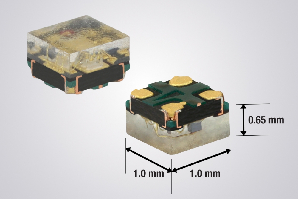
In addition to our SWIR photodetector array, we have developed large-area photodetector sensors for consumer markets. These sensors range in size from 250 µm to 1000 µm, and may be delivered as either bare dies or in standard transistor outline (TO) packages (see Figure 5 for images of these sensors, and a summary of one series of large-area photodetector sensors aimed primarily at operation in the 1300 nm to 1400 nm wavelength band).
One of the strengths of these photodetectors is their dark current density, which can be as low as 8.47 µA cm-2 at room temperature. To investigate the various contributions to dark current performance, we have measured the dark current density for differing photodetector geometries with varying diameters (see the inset of Figure 5 (d)).
We have considered the total dark current density to be a combination of that associated with bulk, and that from surface recombination. Based on this analysis, we have determined that the surface leakage generated during device fabrication is the leading contributor to the dark current of our large-area InGaAs photodetectors. This has led us to conclude that while the performance of our large-area photodetectors is sufficient for many applications, we may be able to introduce improvements as we transition to mature, large-volume manufacturing processes.

Figure 5. Large-area SWIR photodetector sensors for consumer markets. Images of (a) fabricated photodetectors, (b) bare die, and (c) packaged sensors. (d) Bias-dependent dark current data and inset illustrating dependence of dark current density on device geometry to analyse dark current performance
Integration with CMOS
For camera integration, we unite our photodetector arrays with read-out integrated circuits (ROICs) to form focal plane arrays. Traditionally, die-to-die flip-chip bonding, often using indium solder bumps, integrates SWIR photodetector arrays with ROICs. That’s notably different from the approach that’s used with CMOS image sensors, which leverage wafer-scale integration, thanks to wafer size and process compatibility. With our large-diameter wafer platform, we are uniquely positioned to enable wafer-scale integration of InGaAs SWIR photodetector arrays.
There are a number of approaches we have available for wafer-scale integration. We can turn to direct placement die-to-wafer bonding, as well as a direct bond interconnect wafer-to-wafer integration. Both allow us to leverage copper pillar and planar copper-to-copper interconnects, options that outperform indium bumps in terms of energy consumption, bandwidth, and pixel size. Our expectation is that wafer-scale integration will ultimately increase performance while enabling scaling and cost reduction.
The key point to take away is that our InGaAs SWIR photodetector sensors, produced using large-diameter wafers, enable scaling and cost reduction without sacrificing performance. This will help us to address the demand for high-performance SWIR sensors in many markets, including mobile phones, AR/VR, autonomous driving, smart watches, defence and aerospace, industrial automation and machine vision.
But that’s just the start. Our large-scale compound semiconductor platform can also be a game-changer in AI, quantum computing and 5G/6G wireless. How? By enabling quantum-dot lasers for communication and sensing; nonlinear materials integration for quantum communication and frequency conversion; and high sensitivity detection for energy applications.
In short, as well as promising to enhance existing system performance, our technology has the potential to generate new markets not previously envisioned, due to scaling and performance limitations that we now seek to overcome.