Vertical power devices with thick GaN layers on sapphire
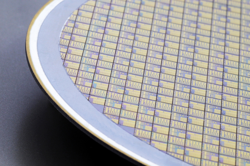
Tuning of wafer bow by stealth laser patterning enables the growth of thick epitaxial layers of GaN on sapphire for vertical high-voltage devices.
BY ELDAD BAHAT TREIDEL, ENRICO BRUSATERRA, FRANK BRUNNER, ALEXANDER KÜLBERG AND OLIVER HILT FROM FERDINAND-BRAUN-INSTITUT (FBH)
µDominating
the headlines of our industry are the vast sums spent on building new
SiC fabs and expanding the capacity in existing facilities. In general, such
efforts are directed at increasing production of 1.2 kV MOSFETs, a key
component in electric vehicles that is helping to maximise their range.
It is beyond question that the
SiC MOSFET outperforms its silicon equivalent. But it could be outclassed by
vertical GaN-based power switching devices, which promise a superior
bang-per-buck.
Leveraging the potential of this class of GaN-based power devices will not be easy – it requires addressing of a number of key challenges. These include: growing a p-n diode on a very thick drift layer that has a well-controlled low doping concentration and supports a high blocking voltage; realising a low forward resistance; and ensuring avalanche capability and short-circuit robustness. Finally, the device heterostructure must be compatible with standard process lines.
Figure 1. Laser grid pattern top view with 30 mm pitch (top
left) and cross-section of the laser damage along one scribe line, resulting in
10 mm of
laser spacial period (bottom left). Illustration of the laser scribing process
(right).
It is not clear what the most
suitable foundation for this device is. While GaN substrates are attractive
from a material quality standpoint, their size is limited to between 50 mm and
100 mm, they come at a high price of around $150 cm-2, and have a
relatively high resistivity, exceeding 1 mΩ cm and going up to 50 mΩ cm. Due to
these limitations, foreign substrates are usually employed for such devices,
with silicon and sapphire being the leading candidates. For both options, the
backside drain contact can be established after either local silicon substrate
removal, or the removal of the sapphire substrate by laser lift-off.
Regardless of the choice of foreign substrate, heteroepitaxy impairs material quality, with GaN suffering from an increased dislocation density. Compounding this concern, a blocking capability larger than 1.2 kV demands GaN epitaxial layers with more than 10 µm thickness, magnifying issues associated with lattice mismatch and differences in the thermal expansion coefficients. These issues include increases in threading dislocation density, leakage current, mechanical strain, fragility and wafer bow.
Figure 2. Optical interferometric bow profile for a range of
wafers with different scribing pitches.
A laser focus
The team at the
Ferdinand-Braun-Institut (FBH) is addressing all these issues with a novel
approach that employs laser patterning. At the 2024 CS Mantech conference,
a technology was unveiled allowing to grow GaN drift layers that are more than
10 µm thick
on 100 mm sapphire substrates. Without further measures the resulting high
wafer bow would make these wafers un-processable on commercial equipment
designed for flat silicon wafers. Progress on this front allowed the
demonstration of fully functional quasi-vertical electronic devices, in the
form of p-n diodes, offering a reverse blocking capability of 1.2
kV.
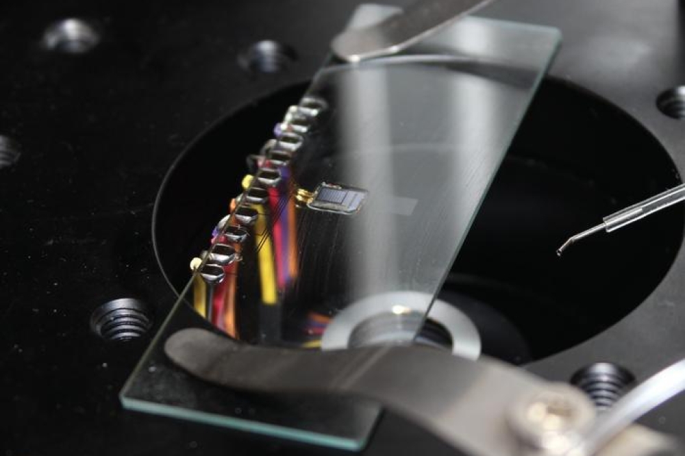
Key for this success was previous work at FBH on using a focused laser beam to reduce the bow of GaN-on-sapphire-based UV LED wafers. To this end, localised damage inside the sapphire substrate, close to its backside surface was created by a tightly focused laser beam. This damage compensates the internal stress that stems from the large lattice mismatch between the epitaxially grown GaN layers and the sapphire substrate.
With this approach it was possible to reduce bow of sapphire wafers with a diameter of 50 mm and an overall thickness of less than 450 µm. However, upscaling of this technology requires extension to larger wafers with even thicker epitaxial GaN layers. Characterisation of 100 mm GaN-on-sapphire wafers with a total GaN layer thickness above 15 µm shows encouraging results.
At FBH we have an industrial process line that tolerates a wafer bow of less than 125 µm, corresponding to a radius of curvature of more than 10 m. However, even with such an accommodating line, wafers with a high bow, but still within process limitations, can still present conformity issues, such as those associated with automated robotic handling, vacuum handling, and uneven temperature exposure.
Our investigations of the impact of laser scribing of GaN-on-sapphire wafers include bow measurements as well as electrical characterization of processed quasi-vertical p-n diodes.
Figure 3. Wafer-level median reverse and forward characteristics for quasi vertical p-n diodes produced on wafers with a different scribing pitch (left). An illustration of the cross-section of a quasi-vertical p-n diode (top right) and a scanning electron microscopy image of such diode (bottom right).
The fabrication of our devices began by loading 650 µm-thick sapphire substrates with a diameter of 100 mm into an MOCVD reactor and depositing a 2.2 µm-thick unintentionally doped GaN transition layer, followed by a 2.4 µm highly conductive n-type GaN bottom layer, and a 10 µm n--GaN drift layer with donor density of 1.4 × 1016 cm-3. The doping concentration of the drift layer was assessed with on-wafer electrochemical capacitance-voltage measurements and post-processing capacitance-voltage measurements. After growth of the drift layer, we added a 530 nm-thick top p-type layer to form a p-n junction and an anode terminal. This structure has a total GaN epitaxial layers thickness of more than 15 µm, and produces an initial wafer bow of around 300 µm, corresponding to a wafer radius of curvature of about 3.8 m if no measures for bow reduction are applied.
Using a fixed focus depth and scribing pitches ranging from 10 µm to 35 µm, these wafers were patterned by focused laser irradiation from the top side through the epitaxial layer stack. The resulting damage is located around 200 µm above the bottom surface of the sapphire substrate. We employed a 532 nm laser with a repetition rate of 40 kHz, using a feed speed of 400 mm s-1 and a continuous laser power of 160 mW, with the focus of the laser inside the sapphire.
The scribing pattern lines are running perpendicular to the flats with the prescribed pitch. Scribing began in the x direction (perpendicular (or parallel) to the main flat), and then in the y direction, with total processing time roughly 4 hours per wafer.
Figure 4. A comparison of the performance of GaN-on-sapphire
quasi-vertical p-n diodes with the ideal breakdown voltage
values.
Perfect pitch?
Optical interferometric bow
profile measurements at different scribe densities revealed that wafer bow
progressively is reduced with decreasing pitch. A smaller scribing pitch
produces a monotonic increase in the radius of curvature, and bow reaches values
as low as around 40 µm,
realised with scribing pitch of 10 µm. Note that the change to the radius of curvature resulting
from laser scribing is inversely proportional to the scribing pitch.
To evaluate the impact of this bow reduction on processability and device performance, we processed quasi-vertical p-n diodes on our line.
We compared devices from wafers with different bow values after laser patterning with different scribe pitch. The reverse-bias off-state current and blocking strength is only marginally impacted by the scribe pitch. In sharp contrast, the onset voltage of our p-n diodes is strongly dependent on the laser scribing pitch. This most probably is related to the strain in the layers that is not accommodated by wafer bow.
Our work shows that the laser scribing of sapphire substrates with thick GaN epitaxial drift layers is a potential route for high-volume manufacturing of 1.2 kV vertical GaN devices on low-cost foreign substrates if the carrier concentration in the drift layer can reproducibly be adjusted to about 1 × 1016 cm-3.
£ This work has received funding from the ECSEL Joint Undertaking (JU), under grant agreement No 101007229. The JU receives support from the European Union’s Horizon 2020 research and innovation programme and Germany, France, Belgium, Austria, Sweden, Spain, Italy.

