Loading...
News Article

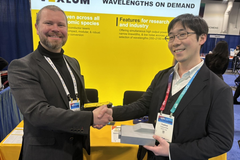
Penn State makes breakthrough in photonic switching

News
Tiny 85 x 85 µm switch can redirect light signals in trillionths of a second

Until now, the photonic switches used for routing optical signals have been hindered by a fundamental tradeoff between size and speed: Larger switches can handle higher speeds and more data but also consume more energy, occupy more physical space and drive up costs.

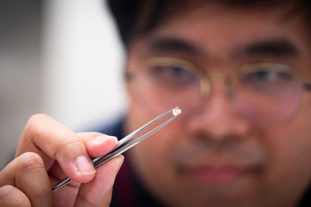
In a new paper in Nature Photonics, researchers at the University of Pennsylvania School of Engineering and Applied Science describe a novel photonic switch that overcomes this size-speed tradeoff. Measuring only 85 by 85 µms, the switch’s units are smaller than a grain of salt but can redirect signals in trillionths of a second.

By manipulating light at the nanoscale, the switch could speed up the process of getting data on and off fibre-optic cables. “This has the potential to accelerate everything from streaming movies to training AI,” says Liang Feng, professor in Materials Science and Engineering (MSE) and in Electrical and Systems Engineering (ESE) and the paper’s senior author.

The switch is a hybrid device with a bottom silicon layer and a top InGaAsP layer that provides optical gain. By tuning the gain level in the top layer, vertically coupled waveguides operate below or above the exceptional point, where light is switched across two layers, among different input–output ports. For a single switching unit, the switching dynamics are of the order of 100 ps.

Joining the two layers proved challenging, and required numerous attempts to build a working prototype. “It’s similar to making a sandwich,” says Feng. "Only, in this case, if any of those layers were misaligned by even a tiny degree, the sandwich would be entirely inedible." The alignment requires nanometer accuracy..

The switch relies on non-Hermitian physics, a branch of quantum mechanics that explores how certain systems behave in unusual ways, giving researchers more control over light’s behaviour.

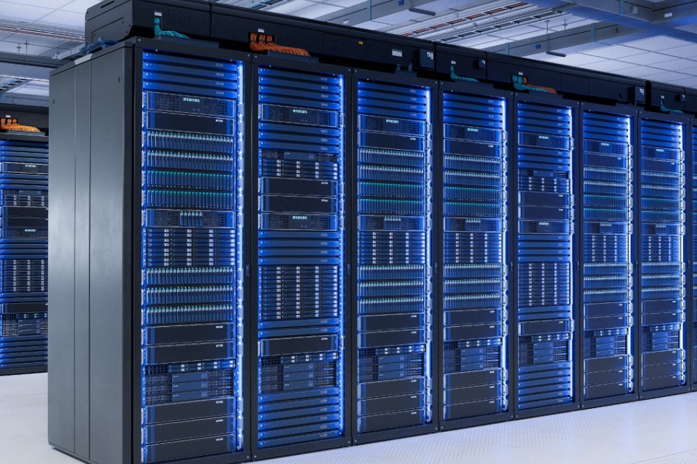
Ultimately, the researchers say, the new switch will benefit not just academic physicists, who can now further explore the non-Hermitian physics upon which the switch depends, but companies that maintain and build data centres, and the billions of users who rely on them.

This study was conducted at the University of Pennsylvania School of Engineering and Applied Science and supported by the US Army Research Office, the Office of Naval Research, and the National Science Foundation.

SPONSOR MESSAGE

Secure Your Hydrogen Supply

A study supply of high-purity hydrogen is critical to semiconductor fabrication. Supply chain interruptions are challenging manufacturers, leading to production slowdowns and stoppages. On-site hydrogen generation offers a scalable alternative for new and existing fabs, freeing the operator from dependence on delivered gas.

Plant managers understand the critical role that hydrogen plays in semiconductor fabrication. That important job includes crystal growth, carrier gas, wafer annealing, and in the emerging Extreme UV Lithography (EUV) that will enable new generations of devices. As the vast need for semiconductors grows across all sectors of world economies, so does the need for high-purity hydrogen.

Take control with Nel on-site hydrogen generation.

Read more
Ascent wins order for power beaming Space PV module
Navitas Partners with Great Wall for 400V-DC power
SemiQ supplies SiC MOSFET modules for EV battery cell cyclers
Coherent and Keysight collaborate on 200G/lane multimode VCSEL tech
Lumentum and Marvell exhibit integrated 450G optical interface
Marktech announces new MWIR LEDS
Imec identifies stable range for GaN MISHEMTs in RF PAs
Polar Light completes $3.4m funding round
Lynred launches advanced thermal imaging modules
Altum RF expands Sydney design centre
Sivers announces partnership with O-Net
Ayar Labs unveils first UCIe optical chiplet
Aixtron delivers InP tool to Nokia
WHU-USTC team demo novel temperature monitoring of GaN device
Phlux lands £9m to take InGaAs sensors to next level
4-inch gallium oxide facility established in Swansea
Mazda and Rohm collaborate on automotive GaN
University of South Carolina chooses MOCVD tool from TNSC
Wolfspeed appoints new CEO amidst funding crisis
SiC slowdown is only short term, says Yole
Pragmatic launches flexible IGZO-based NFC chip
Poet ships latest optical engine samples
EU project to develop 1200V DC powertrain
£250m to turbocharge Welsh compound semi cluster
Scientists harness phonon-polariton electroluminescence
TU Graz team reveals the secrets of heat conduction
Aixtron to partner in ‘GraFunkL‘ UVC project
EU collaboration steps up heterogeneous design
Diodes Inc announces InSb sensors
Far-UVC module targets close-quarters disinfection
Sivers and WIN collaborate on DFB laser production
Boosting the blocking voltage of birectional HEMTs
×
Search the news archive

To close this popup you can press escape or click the close icon.
Logo
x
Logo
×
Register - Step 1

You may choose to subscribe to the Compound Semiconductor Magazine, the Compound Semiconductor Newsletter, or both. You may also request additional information if required, before submitting your application.


Please subscribe me to:


You chose the industry type of "Other"

Please enter the industry that you work in:
 
x
Adblocker Detected
Please consider unblocking adverts on this website