Sivers signs CHIPS Act contracts
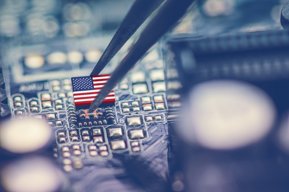
Sivers Semiconductors has signed contracts for both the electronic warfare and 5G/6G chip development awards with the US Northeast Microelectronics Coalition (NEMC) Hub through the US CHIPS and Science Act.
Funding is provided under the Microelectronics Commons program, executed through the Naval Surface Warfare centre Crane Division and the National Security Technology Accelerator (NSTXL).
Sivers says these awards further validate its expertise in wireless innovation around mmWave technology. In these projects, Sivers will work with industry giants like BAE Systems, Raytheon, and Ericsson and lead the charge in commercialising RF and beamforming technology for defence and dual-use applications.
Advance payment of roughly half of the first-year value of both programs is expected to occur by January 2025. If renewed over three years, under the discretion of future awards under the Microelectronics Commons program, the overall funding of both programs is expected to amount to approximately $30M.
“We’re proud to collaborate with our partners on advancing RF technology for 5G/6G FR3 and Electronic Warfare,” said Harish Krishnaswamy, managing director of the Wireless Division at Sivers Semiconductors. “FR3 represents the next leap in cellular innovation, merging the superior range of sub-6GHz with the high-speed capabilities of millimeter-waves. Additionally, we’re excited to broaden our portfolio with cutting-edge solutions for defence and electronic warfare, establishing a strong third pillar for our Wireless Division alongside SATCOM and 5G.”
"Sivers Semiconductors is a key partner as we work to expand microelectronics lab-to-fab capabilities across the Northeast," said Mark Halfman, director, NEMC Hub. "We are excited to collaborate on the development of critical technologies with opportunities for sustainable, positive impacts on our national security."