Improving annealing conditions for GaN MOSFETs
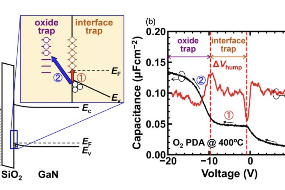
Researchers at Osaka University have demonstrated that low-temperature post-deposition annealing slashes the density of hole traps at the interface between SiO2 and p-type GaN. It’s an observation will aid the development of n-channel GaN MOSFETs, which are promising high-voltage devices.
The tremendous potential of these transistors has spurred extensive studies of interface properties, with investigations of n-type GaN capacitors with a SiO2 dielectric uncovering a gallium oxide interfacial layer that reduces the electron trap density near the conduction band to below 1011 cm-2 eV-1. Thanks to this, mobility in n-channel GaN MOSFETs is more than 100 cm2 V-1 s-1.
However, the reliability of these transistors is impaired by a high density of hole traps near the valence band edge. The density of these traps is so high that p-type GaN metal-oxide-semiconductor (MOS) capacitors tend to exhibit insufficient hole accumulation, and the threshold voltage of MOSFETs shifts during switching. Consequently, to develop highly reliable GaN MOSFETs, it is crucial to quash the density of these hole traps – a task that must begin by uncovering their origin.
The team from Osaka have devoted much effort to this issue. Previous investigations include the use of sub- and above-bandgap illumination to reveal that hole traps have a variety of origins.
Now they are adding to this body of work by studying hole trap generation in GaN MOS structures, with investigations considering a variety of post-deposition annealing conditions for the fabrication of p-GaN MOS capacitors.
To undertake this particular investigation, the team began by taking n-type GaN substrates, loading them into an MOCVD reactor, and depositing a silicon-doped GaN layer with a doping of 2 x 1018 cm-3, followed by a pair of magnesium-doped GaN layers with doping concentrations of 3 x 1018 cm-3 and 2 x 1016 cm-3. Following a wet clean, these samples were annealed under nitrogen for 20 minutes at 800 °C to activate magnesium dopants, prior to a second wet clean and the addition of a 20 nm-thick SiO2 gate dielectric by plasma-enhanced CVD. The researchers completed fabrication of these capacitors with post-deposition annealing for 30 minutes, at temperatures ranging from 200 °C to 800 °C under either oxygen or nitrogen gas, before depositing nickel gate electrodes and aluminium back contacts.
Using the same procedure, the researchers also fabricated n-type GaN MOS capacitors to act as a control.
Comparing capacitance-voltage curves for both types of capacitor produced using an 800 °C post-deposition anneal under oxygen revealed a small hysteresis for the n-type variant, and a large hysteresis for the p-type variant. According to the team, this shows that the p-type structure suffers from strong pinning, due to hole trapping at the MOS interface.
The researchers concluded that post-deposition annealing at 800 °C is ineffective at improving the interface in SiO2/p-GaN MOS structures.
Capacitance-voltage plots were also compared for SiO2/p-GaN MOS capacitors produced without annealing, and with annealing at 200 °C and 800 °C. All the samples produced a large hysteresis, but the one annealed at 200 °C exhibits successful hole accumulation.
To understand the role of the gas used for annealing, the researchers compared capacitance-voltage profiles of SiO2/p-GaN MOS capacitors subjected to a post-deposition anneal under either oxygen or nitrogen at a range of temperatures: 200 °C, 400 °C, 600 °C and 800 °C.
Reseults revealed unusual electron accumulation under forward bias in the nitrogen-annealed samples, and no electron accumulation in oxygen-annealed variants. Regardless of the annealing gas, the team noted hole accumulation in samples with a post-deposition anneal at 200 °C. Higher annealing temperatures under both gases introduced a strong pinning of the surface potential, due to a high density of surface traps.
Following detailed analysis of the capacitance-voltage profiles, the team speculated that the hole trap that causes surface potential pinning is an interface defect, generated at an elevated temperature.
The researchers also noted the presence of high-density oxide traps, even in samples annealed at 200 °C, that trap holes after interface traps are filled.
The team will now focus on the origin of the oxide traps and their reduction.
Pictured above: (a) Schematic energy band diagram of holes trapped in SiO2/GaN MOS structure. (b) Experimental C–V characteristics of MOS capacitor annealed at 400 °C in O2 (black solid line), and second-order derivative calculated using Savitzky–Golay algorithm (red solid line).
K. Tomigahara et al. Appl. Phys. Express 17 081002 (2024)


