Boosting the bang-per-buck with RF integration
The hybrid integration of GaN and silicon paves the way for high-efficiency, cost-effective 5G and millimetre-wave RF systems that provide a cutting-edge power density and scalability.
BY ALEXIS DIVAY FROM CEA-LETI
As demand for data skyrockets, telecommunication infrastructure is being pushed to its limits. To keep up with this growing demand, networks must evolve, not only by increasing their capacity, but by also reducing latency and enhancing global energy efficiency.
One promising solution to improving network performance is to boost data rates by moving to higher-frequency bands. They include the FR3 band, spanning 6 GHz to 24 GHz, and millimetre-wave frequencies between 24 GHz to 40 GHz, a band for 5G applications. However, while these higher frequency bands have the potential to provide faster data transmission and greater bandwidth, they come with a number of new challenges: realising a high energy efficiency; maintaining linearity, key to low distortion; and delivering a robust output power for better coverage and reliable communication.

Figure 1. An example of a heterogenous front-end module: RF
amplifiers benefit from the figures-of-merit of GaN. RF signal generation and
digital parts are in CMOS/BiCMOS.
In this context, the GaN HEMT has emerged as a key
contender. It’s a class of transistor that combines a cutting-edge power
density with a high power-added efficiency, even at millimetre-wave
frequencies, making it ideal for next-generation communication systems.
However, hampering the deployment of the GaN HEMT in the communication sector
is its lack of linearity. This metric is crucial for ensuring that amplified
signals remain clean and undistorted. The degree of linearity directly impacts
communication reliability, especially in high-frequency systems and those
operating with very high modulation complexity.
To address these linearity challenges, engineers tend to turn to techniques such as digital pre-distortion, which compensates for amplifier non-linearities by pre-processing the signal. However, digital pre-distortion requires digital-to-analogue converters, which are not easy to integrate with compound semiconductors, such as GaN. This difficulty causes designs to be more complicated and complex.

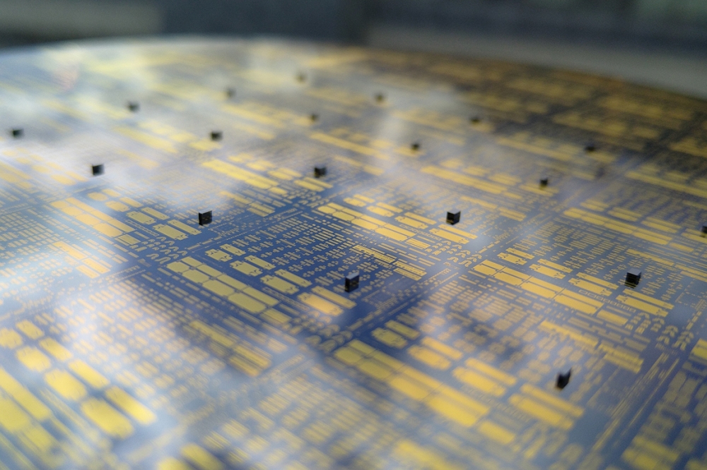
Figure 2. GaN dies stacked on 200 mm silicon RF interposer.
Avoiding these pitfalls are silicon technologies –
particularly CMOS and BiCMOS. They are well-regarded for their ability to
integrate digital and RF functionalities on the same chip. Valuing their
integration are engineers, who benefit from another degree of freedom at the
system level, and are able to design products that feature the co-existence of
front-end RF modules and digital processing circuits. However, silicon-based RF
devices are not a panacea. While highly integrated, they suffer from limitations
in output power and efficiency compared with GaN HEMTs. This trade-off between
power and integration leaves a gap that neither technology alone can fully
bridge.
Merging silicon and GaN
The solution lies in the hybrid integration of GaN and
either CMOS or BiCMOS. By combining GaN RF transistors and silicon-based
technologies, designers leverage the best of both worlds: the high power and
efficiency of GaN for RF applications; and the advanced digital, analogue, and
mixed-signal capabilities of CMOS/BiCMOS. Adopting this hybrid approach opens
the door to more efficient, compact, and powerful systems that can serve a wide
range of applications, from 5G infrastructure and satellite communication to
radar systems and the Internet of Things (IoT).
Moreover, hybrid integration offers a cost-effective path forward. By stacking GaN RF transistors only on top of silicon RF and digital circuits, manufacturers can avoid high costs associated with large-area GaN chips. GaN die are significantly more expensive than silicon, so reducing the amount of GaN material while still benefiting from its performance can lead to significant cost savings. However, assembling these technologies in a tight space presents its own set of challenges, particularly at high frequencies.

Figure 3. (left) Transistor ready for pick and place
assembly (right). Future package heatsink emulation using a copper finger,
allowing higher electrical performance.
When working at frequencies of several gigahertz or more,
traditional assembly methods like wire bonding are inefficient, introducing
signal losses that degrade performance. However, it’s now possible to eliminate
these connections, thanks to recent advances in 3D integration technologies
that enable high-density integration of CMOS and III-V (GaN) transistors on the
same chip. The upshot is lower parasitic losses, improved signal integrity, and
faster signal transfer – all critical for high-performance RF systems.
Several solutions have been developed for integrating GaN and silicon technologies, with copper pillars and hybrid bonding offering the most promise. The latter, which involves bonding at the wafer level, requires a back-end process that is fully compatible with CMOS technology, limiting its use to CMOS-compatible GaN processes. Meanwhile, copper pillars offer greater versatility, but their use with GaN-on-SiC technologies remains challenging, due to material and process complexities.
Recently, a variety of heterogeneous integration schemes have been proposed and tested, often involving sophisticated and unconventional processes. Looking to improve on this, our team at CEA-Leti has developed a simpler, more cost-effective approach. We begin by processing a GaN HEMT on a large-format silicon substrate using industrial processes and copper pillar growth, before dicing and stacking GaN devices on a silicon interposer. These steps ensure a performance that is close to the state of the art, crucially realised with a more scalable and economical process.
Our hybrid integration of GaN and silicon opens up exciting possibilities for the future of RF communication systems. By combining the strengths of both these technologies, we create systems that not only excel in power and efficiency, but are cost-effective and scalable. This makes our approach to hybrid integration of GaN and silicon an ideal one for meeting the growing demands of 5G, satellite communication, and serving in applications beyond that.

Figure 4. (left) Schematic of the demonstrator’s
architecture, featuring two GaN transistors stacked on co-planar waveguide
transmission lines through 25 µm height and width copper pillars. (right)
RF performance of the stacked transistor. Thermal dissipation is mandatory for
higher voltages/power densities.
Cutting-edge RF technology
For more than a decade, scientists around the world have
been striving to advance GaN-on-silicon technologies. Their motivation includes
lower chip costs, increased volume, and the advantages that come from using 200
mm and 300 mm cleanroom tools. Offering enhanced process control, these more
modern machines significantly reduce chip-to-chip variability and enable more
reliable and efficient semiconductor devices. Our institution is a leader in
this field, developing cutting-edge power and RF GaN HEMTs on 200 mm silicon
substrates. These devices hold great promise for the next generation of
high-frequency and high-power applications.
At the heart of this development is an RF GaN device, based on AlGaN/GaN epilayers grown on a high-resistivity 200 mm silicon <111> substrate. This high-resistivity substrate minimises RF losses to 0.27 dB mm-1 at 30 GHz, measured using coplanar waveguides at the final stage of the HEMT process. These minimal RF losses are critical for ensuring the overall efficiency of the amplifier, making this technology a strong contender for the future of RF systems. The relationship between RF losses and amplifier efficiency is well-known, as lower losses directly contribute to higher overall performance in high-frequency circuits.
The fabrication process for making these GaN HEMTs is fully CMOS-compatible and gold-free, ensuring integration with standard silicon manufacturing processes. Multi-finger transistors with coplanar access are produced using a TiN Schottky gate with a 150 nm gate length. The specific device discussed here has four fingers and a 50 mm gate width.
For this GaN-on-silicon transistor, operating at a current density of 1.35 A mm-1, the cut-off frequency (fT) is 83 GHz and the maximum oscillation frequency (fMAX) 220 GHz. These are very encouraging frequencies for millimetre-wave applications, particularly those at 30 GHz, because the value for the maximum oscillation frequency is more than five times higher than the target operating frequency. This substantial margin ensures that the device offers high gain and excellent efficiency at millimetre-wave frequencies, making it ideal for 5G millimetre-wave and beyond-5G applications.
We have measured this device’s large-signal performance at 28 GHz – a key frequency for 5G millimetre-wave communications – testing the GaN transistor in class AB operation. Under these conditions, and a nominal bias of 10 V, our device delivers an output power of 26.5 dBm at a power-added efficiency of 43 percent. When we double the initial bias to push the device harder, the power density climbs to 4 W mm-1, translating to nearly 1 W of output power (29 dBm). This high power-density underscores the strength of GaN-on-silicon technology in handling the demands of high-frequency, high-power applications while maintaining efficiency.
For ease of testing, and to demonstrate the potential of 3D integration, we have stacked our GaN chiplets on a silicon substrate. We left our bottom silicon substrate as a passive interposer, featuring RF pads and coplanar waveguides, to facilitate connections to the flip-chipped GaN chiplet, which we bonded using copper pillars. We built the RF passive interposer, developed specifically for 3D RF system characterisation, on a trap-rich high-resistivity (2 kΩ cm) silicon wafer that’s designed to minimise RF losses.
This high-resistivity silicon substrate helps us to address a common issue in silicon-on-insulator processes: parasitic surface conduction. With our configuration, the trap-rich design slashes this conduction, leading to lower losses and superior linearity of passive devices on the substrate. These benefits are critical for maintaining the high performance needed for RF systems, particularly at millimetre-wave frequencies.
To ensure precise measurement and calibration, our interposer design includes multiple thru-reflect-line calibration kits. These kits, along with various footprints designed to accommodate 3D GaN dies with widths ranging from 500 µm to 1 mm, ensures that our system can support future developments in GaN technology. The interposer’s access lines have RF losses of less than 0.25 dB mm-1 at 28 GHz.
Interconnect performance
To ensure optimal performance in high-frequency GaN devices,
interconnections between the GaN chip and the interposer have to strike a
delicate balance. On the one hand, these connections must be short enough to
minimise parasitic effects – specifically resistance and inductance. These
parasitics threaten to degrade signal quality and impair overall system
efficiency, especially at higher frequencies. However, on the other hand, it’s
essential to position the GaN chip far enough from the interposer to prevent
electromagnetic compatibility issues, which can disrupt signal integrity.
For our demonstrator, we employed copper pillars to realise the ideal interconnection height, while addressing both parasitics and electromagnetic compatibility concerns. We fabricated our pillars by electrochemical deposition on both the silicon substrate and the GaN wafer. To ensure robust electrical connections, we finished the GaN wafer with a tin-silver coating, a standard material for solder joints in advanced packaging. After growing our pillars, we carried out a solder reflow process on the GaN wafer to prepare the bumps for assembly. We then diced the GaN wafer into individual chips, which we precisely positioned using a pick-and-place machine. Finally, we used a second solder reflow to complete the 3D assembly. This process led to an interconnect height of 25 μm, with a pitch (the spacing between pillars) matching the same dimension, ensuring compact yet efficient connections between the GaN chip and the interposer.
A key aspect of our development process has been the rigorous testing of the copper pillar interconnects under millimetre-wave conditions. We performed several RF measurements, considering both standard 2D transmission lines and daisy chains featuring copper pillars. These tests confirm the low-loss characteristics of the interconnects, showcasing insertion losses below 0.05 dB per 3D transition at 28 GHz using coplanar waveguides.Such minimal losses are significant at millimetre-wave frequencies. This level of performance ensures that multiple transitions – such as those at a transistor’s input and output – can be incorporated without a substantial degradation in efficiency or signal quality. In practical terms, this opens the door to a higher degree of integration in GaN-based systems, allowing for more compact designs that do not compromise performance.
3D-GaN RF performance
When a GaN transistor is integrated atop a silicon
interposer, it does not behave in the way it does in its native 2D
configuration. While interconnect height and placement are optimised to reduce
electromagnetic interference and minimise signal losses, thermal management
becomes a critical challenge, especially when the transistor operates in power
amplifier mode.
One of the first noticeable differences in resulting from the stacking of the GaN transistor is its higher thermal resistance compared with the 2D version. According to DC characterisation, current levels fall by around 20 percent when the device is handling a high dissipated power, a clear sign of thermal limitations. Under small-signal conditions – with S-parameter measurements taken up to 67 GHz – the device suffers from self-heating. Even at modest bias points, the transistor’s temperature is higher by at least 75 °C than the chuck temperature. This substantial increase in temperature stems from the relatively high junction-to-chuck thermal resistance in the 3D configuration, which restricts heat dissipation to through just the copper pillars that connect the GaN chip to the silicon interposer.
Despite these thermal limitations, our GaN transistor delivers a solid RF performance. At 28 GHz under large signal operation, it produces a power density of 2.2 W mm-1 at nominal voltage with a 41 percent power-added efficiency, showing minimal gain degradation. However, as the voltage increases, the self-heating effect becomes so severe that it causes the amplifier’s performance to deteriorate significantly.
To tackle these thermal challenges, we have implemented an innovative but straightforward solution. This involves placing a copper finger that’s coated with thermal grease on the backside of the GaN chip, emulating a future package with a dedicated thermal sink. This addition allows heat to dissipate more effectively by conduction, improving the RF performance and bringing it much closer to its original efficiency.
Turning to this heatsink has enabled us to halve DC performance degradation and recover almost 90 percent of the performance seen in the ideal 2D configuration, which operates on a thermal chuck. Small-signal gain shows only a 0.32 dB drop compared with the ideal case, and large-signal performance improves dramatically. Once again, our device delivers a power density of 4 W mm-1, matching its performance in the 2D configuration, with no observed degradation during testing. We conclude that this simple thermal management strategy is highly effective, allowing nearly 1 W of output power to flow through the interconnects without performance loss.
In addition to addressing thermal concerns, our chiplet integration of GaN with silicon offers several key benefits. One of them is that by employing a die-to-wafer bonding process, manufacturers can implement a ‘known good die’ approach, significantly boosting system yield. This merit has much value, given the lower yields typically associated with GaN technologies compared with high-volume 300 mm silicon CMOS/BiCMOS processes. Another advantage of our approach to integration is that it uses only the necessary GaN components, rather than an entire GaN-on-SiC MMIC, enabling a reduction in the overall GaN footprint used in a given front-end module or RF system, leading to substantial cost savings.
However, there are still challenges. Amongst them, one of the most significant is the low pick-and-place machine assembly speed for small dies – that is those with a width below 1 mm. Our colleagues at CEA-Leti are currently working on this issue, which must be resolved to obtain a competitive solution.
Looking ahead, our plan is to introduce additional design improvements that will focus on minimising impedance mismatches in the 3D configuration to ensure optimal RF performance. We are also aiming to undertake advanced 3D thermal simulations to refine the design guidelines for heterogeneous GaN-CMOS/BiCMOS power amplifiers utilising copper pillar technology.
In parallel, we will continue to develop new GaN demonstrators delivering an enhanced performance. These future designs will feature advanced AlN barriers and MIS gates that push power density even further, to exceed 6 W mm-1 – a level previously only realised with GaN-on-SiC devices. By leveraging these innovations, our GaN-on-silicon technology is poised to bridge the performance gap with SiC, while offering the cost and integration benefits of silicon. It’s an approach that’s paving the way for next-generation high-efficiency RF systems.