
Terahertz light controls atomically thin semiconductors
Physicists at Bielefeld University and the Leibniz Institute for Solid State and Materials Research Dresden (IFW Dresden) have developed a method to control atomically thin semiconductors using ultrashort light pulses.
The study published in Nature Communications could pave the way for components that are controlled at unprecedented speeds directly by light.
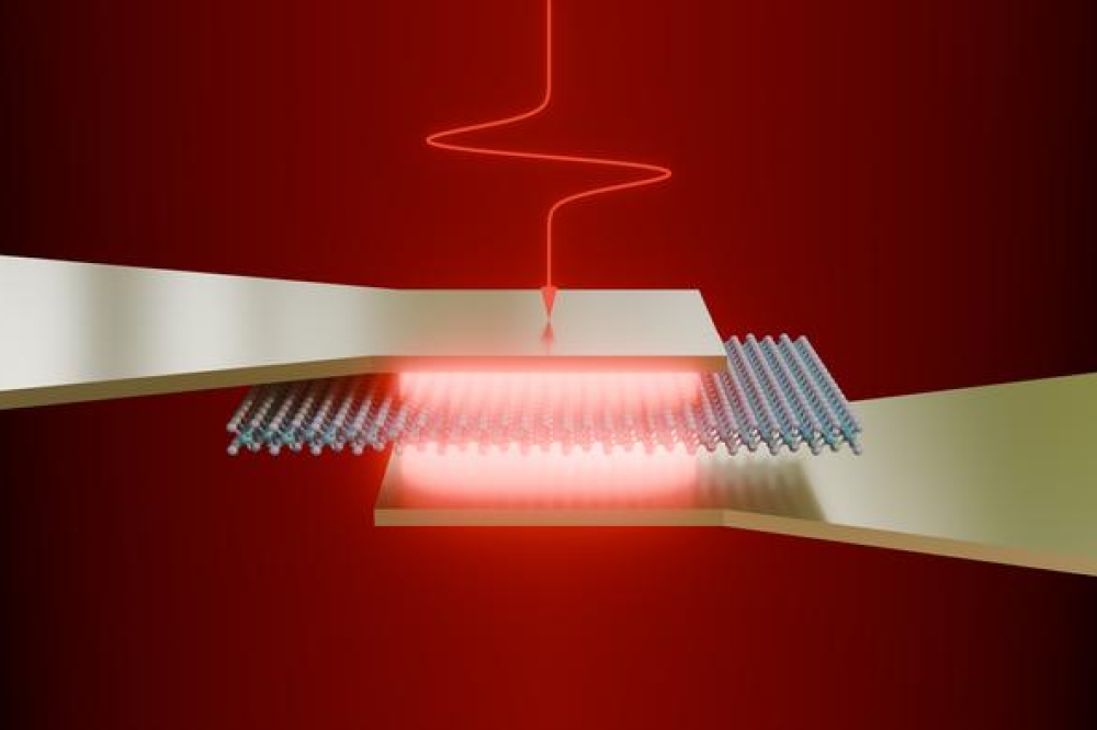
The researchers employ specially designed nanoscale antennas to convert terahertz light into vertical electric fields in atomically-thin semiconductors, such as MoS₂. These electric fields reach several megavolts per centimetre strength.
‘Traditionally, such vertical electric fields, used, for example, to switch transistors and other electronic devices, are applied using electronic gating, but this method is fundamentally limited to relatively slow response times,’ explains the project leader, physics professor Dmitry Turchinovich from Bielefeld University. ‘Our approach uses the terahertz light itself to generate the control signal within the semiconductor material – allowing an industry-compatible, light-driven, ultrafast optoelectronic technology that was not possible until now.’
Ultrafast material control
The technique allows real-time control of the electronic structure on timescales of less than a picosecond. The scientists were able to experimentally demonstrate that the optical and electronic properties of the material could be selectively altered using light pulses.
The fundamental concept, along with the experimental implementation and theoretical modelling, was developed at Bielefeld University. Tomoki Hiraoka, lead author of the study and a Marie Skłodowska Curie Fellow in Turchinovich’s group at the time, played a key role in the project. "Seeing such a strong and coherent effect induced purely by terahertz light pulses was very rewarding," says Hiraoka.
The complex 3D–2D nanoantennas necessary to produce this effect were fabricated at IFW Dresden by a team led by Andy Thomas. ‘It took us a lot of work to develop the optimal devices — we had to fabricate and test many different structures before achieving the desired performance,’ says Thomas.
The researchers think the development could lead to ultrafast signal control devices, electronic switches, and sensors. Such components are used in data transmission, cameras, and laser systems. Potential application areas include communication systems, computing, imaging, and quantum technologies.
Reference
Hiraoka, T., Nestler, S., Zhang, W. et al. Nat Commun 16, 5235 (2025


