
Robust supercrystals for the LEDs of the future
Nanometer-sized crystals of perovskite offer great potential for applications in the field of LEDs, solar cells and optical switching elements. A particularly interesting arrangement occurs when a large number of these nanocrystals join to form a larger structure – a supercrystal.
Researchers at the University of Tübingen have now found a novel way of achieving this which has produced perovskite supercrystals that are particularly stable. They have presented their findings in the journal ACS Nano.
Perovskite nanocrystals are an exciting area of research, explains Jonas Hiller from the University of Tübingen, one of the authors of the study. “Their optoelectronic properties depend heavily on their size – which is typical of quantum behaviour,” explains Jonas Hiller from the University of Tübingen, one of the authors of the study. “Because of this, their properties can be specifically customised. The energy of the light they absorb or emit varies depending on their composition and their size.”
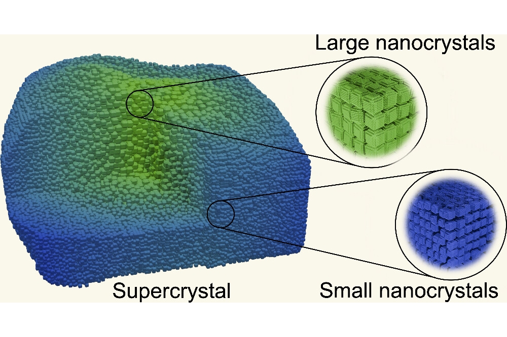
Under certain conditions, these perovskite nanocrystals can form larger structures, creating a supercrystal. “The exciting thing is that while the individual nanocrystals retain their desired quantum properties, they can be handled as a macroscopic unit and thus deployed in practical applications," says Hiller.
Until now, supercrystals like this have been created by allowing a solvent containing the perovskite to slowly evaporate. The resulting structures form very gradually on the substrate. “However, the supercrystals are produced at random sites around the substrate,” explains the project manager Ivan Zaluzhnyy from Tübingen. “Also, the individual nanocrystals are surrounded by a protective layer of organic molecules which makes the entire supercrystal very soft.” As a result, they break very easily when you try to move them around mechanically. This poses a real obstacle for applications in which the positioning of the materials is crucial, such as between two electrodes in an electrical component.
To solve this problem, the team opted for an alternative approach: two-phase diffusion. A solution containing the nanocrystals is layered on top of a second liquid: acetonitrile. This acts as an anti-solvent for the perovskite crystals. As it slowly penetrates the solution containing the nanocrystals, it gradually reduces their solubility. “This results in crystal growth beginning at the boundary surface between the two phases,” explains Hiller. The acetonitrile displaces the organic molecules coating the crystals, resulting in a firmer, more stable structure.
In order to examine the structure of these supercrystals more closely, the team used a narrow bean X-ray source at PETRA III, at DESY (the Deutsches Elektronen-Synchrotron).
“The beam diameter of just 300 nanometres makes it possible to examine different regions within a supercrystal with high precision,” explains DESY physicist Wojciech Roseker. And Hiller adds: “The extremely high quality of the diffraction data was a key element of this study. It enabled us to analyse the structure of the supercrystals in great detail.”
The team found that the supercrystals produced, typically had an area of 10 by 10 square µm but were significantly thicker than the comparatively flat structures that could be achieved using the old method. Their height was more than 5µm which improves their stability. They say this makes the supercrystals robust enough to be gripped with micromanipulators and moved to other locations – a first for perovskite structures.
Reference
Jonas L. Hiller et al; ACS Nano 2025, 19, 28, 26117–26126


