Making incompatible materials compatible
Researchers from Fraunhofer ISE in Germany, the University of Sherbrooke in Canada, the University of Michigan in USA, and Université Paris-Saclay in France have developed a novel way to integrate high-quality germanium layers on silicon. The post-epitaxial approach uses a nanometer-scale 'free surface' between the epilayer and the substrate.
By enabling nearly defect-free germanium layers on low-cost silicon substrates, the method paves the way for cheaper, more efficient multi-junction solar cells, integrated photonic circuits, and high-performance sensors, according to the team.
Moreover, it addresses one of the fundamental challenges in semiconductor manufacturing — how to combine materials with very different lattice constants without introducing performance-killing defects.
For decades, engineers have struggled with integrating lattice-mismatched materials like germanium, III-V alloys, and silicon. The difference in atomic spacing creates strain that leads to dislocations, severely impacting electronic and optical properties.
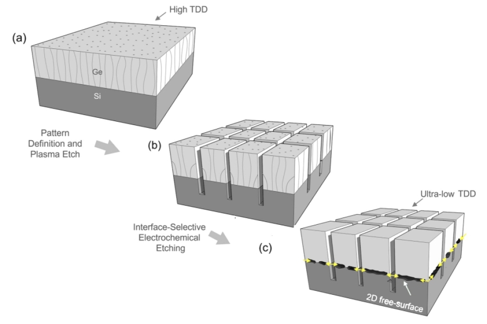
Previous strategies typically relied on thick buffer layers or costly substrates, which add complexity and expense. In contrast, the new technique — described by the team as “germanium on quasi nothing” — introduces an ultra-thin, ~1 nm interface that decouples the active layer from its substrate. This tiny gap acts like a mechanical cushion, allowing the layer to relax and heal most of its crystal defects.
The researchers used epitaxial growth techniques to deposit germanium on silicon while engineering this delicate 2D free surface. Transmission electron microscopy revealed a striking reduction in dislocation density, with the germanium layer exhibiting nearly bulk-like crystallinity. Atomic force microscopy confirmed an atomically smooth surface, making it ideal for subsequent device processing. Electrical and optical measurements also showed promising performance, indicating that this approach could rival traditional bulk Ge substrates in many applications.
Looking ahead, the team plans to adapt the same concept to other material systems, such as GeSn/Si and InGaAs/Si, to enable new types of photonic and quantum devices. They also aim to integrate III-V junctions directly on silicon to build next-generation multi-junction solar cells with dramatically reduced costs. The generality of this 2D free-surface engineering opens exciting possibilities across microelectronics and optoelectronics.
Pictured above: a) Heteroepitaxial growth of a bulk Ge film on a (001) Si substrate, resulting in high density of threading dislocations (TDD) due to lattice mismatch. b) Formation of exposed sidewalls via Deep Reactive-Ion Etching (DRIE), followed by cyclic annealing. c) Introduction of an interfacial 2D free surface by selective electrochemical etching.
Reference
Y. A. Bioud, M. Bouchilaoun, W. Schreiber, et al; Adv. Mater. (2025)