
Sealing tech to balance performance, maintenance and lifecycle value

Greene Tweed’s high-performance seals enable compound semiconductor manufacturers to thrive in a volatile market by optimising the total cost of ownership while providing robust protection against harsh processing conditions.
BY ALAN MAHER AND PRAGATI VERMA FROM GREENE TWEED
The compound semiconductor industry is entering a period of promise and disruption. Sales are projected to hit $25 billion by 2030, spurred on by an average annual growth rate of almost 13 percent, according to semiconductor market research analyst Yole Group. What is fuelling this surge? It’s the booming demand for GaN and SiC, driven by the rise of electric vehicles, 5G networks, and renewable energy tech.
While this growth is welcome, it comes with challenges. There’s a backdrop of tightening global regulations, fluctuating tariffs, export bans and geopolitical tensions – factors that disrupt the supply of GaN and SiC. And on top of that, there’s the cyclical nature of market demand, threatening to turn forecasts upside down.
For businesses in this space, managing risk and profitability often comes down to one question: how do we enhance our operations while controlling costs, especially amidst volatility?

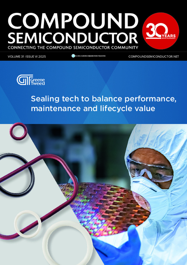
High-performance Fusion seals, built to withstand extreme temperatures,
high pressures, corrosive chemicals, and volatile fluids.
Why cost-of-ownership matters in uncertain times
One of the keys to thriving in an unpredictable market is to give a lot of consideration to the total cost of ownership for compound semiconductor manufacturing tools and processes. The production of compound semiconductor epiwafers and devices tends to require specialised equipment, unique materials and complex processing steps, all of which drive up initial investment and ongoing operational costs.
Due to all these factors, manufacturers must look beyond upfront costs of major equipment to consider long-term expenses associated with even the smallest components, such as the elastomeric seals in their equipment and tools.
At Greene Tweed, we assist with this task by engineering sealing solutions that outperform and outlast in the world’s harshest semiconductor manufacturing applications. Many prominent chipmakers depend on our portfolio of perfluororoelastomer (FFKM) Chemraz and fluoroelastomer (FKM) Fusion seals to manufacture silicon and compound semiconductor devices.
As the total cost of ownership becomes a central concern, our portfolio of advanced seals strikes the ideal balance between performance, maintenance, and lifecycle value. By focusing on enhancing maintenance cycles and ensuring higher equipment uptime, our seals help compound semiconductor manufacturers realise better yields and profitability, even during challenging times. The crucial balance between performance, maintenance, and lifecycle value is even more crucial for tools and processes exposed to extreme plasma and chemical environments, such as those found in etching and deposition chambers, where seals often bear the brunt of these costs. Faulty or inefficient seals are highly detrimental, as they can lead to equipment failures, unplanned downtime, and ultimately suboptimal yields.

For compound semiconductor fabs, Chemraz G-Series prevent contamination while withstanding aggressive conditions.
When it can’t fail
To understand the critical importance of seals in the compound semiconductor industry, consider the pendulum valve. Located inside etch and deposition chambers in fabs, it is an indispensable component in compound semiconductor manufacturing processes involving 200 mm wafers. The roles of these sophisticated valves are to regulate critical gas flow and help maintain the vacuum conditions required for precise wafer processing. Success on these fronts ensures efficient etching or deposition.
The performance and the longevity of pendulum valves heavily relies on their seals. Harsh chemicals and plasma environments can rapidly degrade seals, leading to erosion, sticking, and cracking. Seal quality can also diminish through constant dynamic motion, such as compression, decompression, and rotation, as this creates friction, accelerates wear and reduces lifespan. Add the extreme heat from wafer fabrication, and challenges faced by seals skyrockets. Even the smallest of failures can disrupt valve operation, leading to costly delays, unplanned downtime, and expensive repairs.
The good news is that our high-performance seals, such as Fusion – and in particular Fusion F07 – are built to withstand extreme temperatures, high pressures, corrosive chemicals, and volatile fluids. These strengths enable manufacturers to improve the performance and the lifespan of their pendulum valves in demanding vacuum applications.
But what happens if a seal in a pendulum valve fails? The consequences are dire, as the entire valve goes down with it. One ramification is that the vacuum needed for wafer processing collapses, leading to chamber contamination and ruined wafers. There’s also the distinct possibility of a catastrophic chain reaction, involving material scrapping, production delays, and equipment damage. Persistent failures can even destroy other high-cost components or compromise the entire tool, sending repair costs through the roof. What’s abundantly clear is that seal reliability is a non-negotiable, ensuring that these valves perform flawlessly during semiconductor plasma processing.

Located inside etch and deposition chambers in fabs, pendulum valves regulate critical gas flows and help maintain vacuum conditions required for precise wafer processing.
Fusion: Balancing performance and costs
Pendulum valves aren’t alone. There are a number of tools and processes, including lid seals and slit valve seals in fabs, that rely on our Fusion sealing solutions to deliver certainty during crucial operations.
Engineered to bridge the gap between performance and cost, Fusion F07 is a dependable FKM solution that’s tailored for the compound semiconductor and legacy semiconductor market. The material used to produce this seal ensures an ideal balance between affordability and chemical resistance, making F07 a natural choice for 200 mm and smaller wafers widely used to make a vast range of compound semiconductor devices. Operating continuously at temperatures of up to 180 °C, and including excursion service temperatures of up to 220 °C, F07 has a minimum expected lifetime of six months, outperforming standard FKM seals in these applications. Additionally, F07 has a lower total-cost-of-ownership than a number of premium materials, making it an economical yet high-performing solution.
Developed specifically for CVD and dry plasma etch equipment that’s used in the manufacture of flat panel displays, the 707 family of seals ensures exceptional chemical resistance while maintaining reliability and minimising contamination. For plasma equipment applications, there’s also the Fusion 706, a versatile option that handles everything from etch and plasma-enhanced CVD to plasma ashing processes. Note that the 706 is also suitable for systems requiring low sealing force materials, such as bonded slit valve gates.
Our Fusion products can assist with efforts to trim chip production costs by upgrading from 150 mm to 200 mm wafers. Compared with the production of silicon devices, manufacturing those that are based on compound semiconductors, such SiC, is inherently more expensive, due to high material costs, complex processes, and lower yields. Many companies aim to cut expenses by retrofitting older tools with software and component upgrades, instead of investing in entirely new equipment. For these efforts, we offer upgraded seal kits, to enhance the performance of outdated tools.
By integrating advanced sealing solutions, these chipmakers can optimise older refurbished equipment, preventing contamination and maintaining cleanroom standards. As well as increasing throughput and yield, this approach supports the growing demand for compound semiconductors while maximising profitability.
Chemraz: Outperforming in the harshest conditions
Manufacturers of compound semiconductor devices often operate in incredibly demanding industrial conditions, which may involve extreme temperatures, aggressive chemicals, and a plasma environment. These conditions place significant stress on seals and other components. In such applications, prominent chipmakers tend to turn to our Chemraz FFKM seals to prevent contamination while withstanding aggressive conditions. These seals play a critical role in chip production, where anything less than the best simply won’t do.
For compound semiconductor fabs managing legacy equipment for chip production, the Chemraz G-Series delivers exceptional versatility, and the performance needed to meet demanding manufacturing challenges. This FFKM material is engineered to excel in aggressive plasma chemistries and dynamic sealing applications, making it a reliable choice for demanding manufacturing environments.
The Chemraz G-Series stands out for its superior plasma resistance, performing reliably in oxygen and fluorine-rich environments. Its ability to withstand such harsh conditions ensures consistent performance, even in the most demanding applications. Whether used as a door seal or an actuator O-ring, Chemraz significantly reduces particulation while boosting operational uptime, contributing to smoother and more efficient manufacturing processes.
Working in tandem, the Chemraz FFKM and Fusion FKM series provide a complete range of sealing solutions for compound semiconductor manufacturers. Designed for both legacy systems and the latest tools, these materials offer the durability and flexibility needed to support every stage of production. The goal is simple: ensuring efficiency and reliability throughout the entire manufacturing process.
If you are searching for the right seal for your application, Greene Tweed’s Elastomer Selection Guide makes it very easy by simplifying the process of choosing the most suitable seal for every application. This proven process considers key factors, such as material compatibility, seal geometry and operating conditions, to develop solutions tailored to the specific needs of semiconductor manufacturing. By aligning seal types with precise engineering criteria, the Right Seal Pyramid methodology addresses key challenges, like chemical resistance, mechanical stress and installation accuracy, to ensure reliable performance in the harshest semiconductor manufacturing environments.
Prepare for the next upswing
Selecting the right components and optimising the total cost of ownership can pay dividends in an uncertain market. After all, the cyclical nature of the semiconductor industry is no secret. While the timing and breadth of these cycles are increasingly difficult to predict, it is critical to be ready for the next upswing. Navigating uncertainty, whether from tariffs, supply chain shocks or technological disruption, demands strategic investment in the right materials and designs for components such as seals.
For over 160 years, our company, Greene Tweed, has been applying our expertise in materials science and engineering to support innovation in the industries we serve.
By focusing on reliable processes, high-quality sealing solutions and advanced technologies, we are helping semiconductor manufacturers improve their operations and scale efficiently.
Our support plays a key role in fostering long-term growth and ensuring the reliability of critical components in the semiconductor industry.
As the compound semiconductor industry braces for a year of typical shifts and unpredictable headwinds, one thing is clear. In this environment, those taking a strategic approach to managing the total-cost-of-ownership by factoring in not just purchase price but also the reliability, flexibility, and resilience of small indispensable components, such as seals, will be better positioned to weather volatility and maintain profitability.


