

Powering quantum and space technologies
Cutting-edge power devices are performing in the coldest environments ever tested, unlocking new possibilities for space exploration, quantum computing, and energy systems.
BY XIN YANG, ZINENG YANG AND YUHAO ZHANG FROM THE UNIVERSITY OF HONG KONG AND LINBO SHAO FROM VIRGINIA TECH
In the shadowed craters of the Moon, inside quantum computers, and within futuristic superconducting power grids, electronics faces a common enemy: extreme cold. Temperatures below 4 Kelvin, that’s less than -269 °C, are not just harsh – they’re a fundamental barrier. When exposed to these conditions, most materials grind to a halt, with electrons ‘freezing’ in place and refusing to move. Yet, these frigid environments are precisely where tomorrow’s technologies will thrive.
For quantum computers, temperatures that are very close to absolute zero are needed to stabilise qubits. Incredibly low temperatures will also be endured by spacecraft sent to explore Pluto or Mars, with electronics having to survive -230 °C. And futuristic energy grids, relying on superconducting cables, will demand power converters that operate in the cold. Until now, one critical question has lingered: Can power semiconductors – the backbone technology of energy conversion – function in these extremes?

Figure 1: Reported cryogenic studies of (a) GaN power HEMT, (b) SiC MOSFET and (c) silicon IGBT, highlighting the unexplored range in the prior literature. The lowest temperature, research institute, and year of each report are marked. Studies are grouped into the static low-voltage (LV) test, breakdown voltage (BV) test, dynamic on-resistance (D-RON) test, and dynamic switching (SW) test. The lowest temperature for device characterisation in this work is marked in star symbols for different types of tests.
Answering this question is the groundbreaking study by our team from Virginia Tech and the University of Hong Kong. We have been testing silicon, SiC, and GaN power devices down to 0.1 K, which is colder than the vacuum of space. These investigations have provided the first ever insight into how power devices perform deep within the cryogenic regime, using evaluations based on switching tests and static characterisations (see Figure 1). Our results, obtained using tools employed in quantum physics research, reveal a new frontier for power electronics.
Breaking the ice
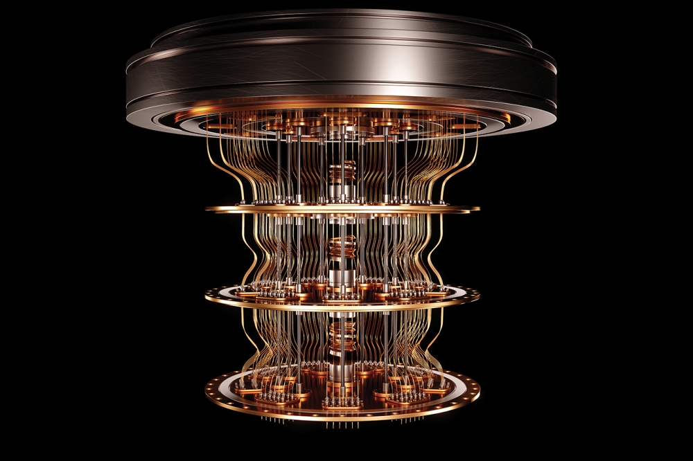
Our investigation has involved the use of a dilution refrigerator, originally designed for quantum physics experiments, and repurposed for power electronics testing (see Figure 2). Unlike conventional refrigerators, our high-tech ‘freezer’ uses helium isotopes to cool samples to 0.1 K – a staggering 10,000 times colder than liquid nitrogen.
The cooling process begins with a pulse tube cryocooler, lowering the temperature to 3 K using helium gas. The dilution unit then takes over, leveraging a quantum cooling mechanism where helium-3 and helium-4 isotopes separate into two phases below 0.87 K, with helium-3 extracting heat as it moves between them. The mixing chamber, the coldest point at 10 mK, serves as the mounting location for test devices.
Adapting this system for power electronics, which operate at high voltages, high currents, and fast switching speeds, posed a number of challenges, including increased measurement noise and potential thermal instability.
To overcome them, we engineered a custom setup, featuring: a daughter board mounted at 10 mK; superconducting cables to carry high currents without resistance; and a dynamic test circuit, to simulate real-world switching conditions. Using this setup, we undertake reliable performance evaluation in extreme cold.

Figure 2: (a) Photograph and (b) an illustration of a cryogenic test
setup, which consists of a BlueFors dilution fridge, a Keysight B1505
curve tracer, and a customised circuit test setup. The daughter board
with the device under tests (DUTs) is mounted on the 10 mK plate, and
other components and equipment are placed outside the fridge.
To accurately assess the performance of power semiconductors at cryogenic temperatures, we use two complementary measurement systems: a dynamic switching test and static current-voltage sweeps. For our double-pulse test, we pulse devices on and off within microseconds, allowing us to capture turn-on/off speeds and dynamic resistance with high precision. To combat signal distortion, we use a noise-cancelling model to filter out cable-induced interference.
For measurements of steady-state characteristics, we connect a Keysight B1505A curve tracer to the dilution fridge. This instrument maps voltage thresholds, leakage currents, and breakdown limits of devices at 0.1 K. To prevent thermal instability, we limit the maximum test current to 1 A.
We have tested three industry-standard power devices rated at 650 V: a GaN HEMT, a SiC MOSFET, and a silicon IGBT. As well as spanning three mainstream power semiconductor materials, this selection included both unipolar and bipolar devices.
Our ultimate goal has been to determine whether these devices block high voltages, switch efficiently, and avoid catastrophic failure in the extreme cold – essential for future cryogenic power systems.
GaN: The cryogenic champion
Among the three classes of device tested, the GaN HEMT demonstrates remarkable performance improvements at cryogenic temperatures (see Figure 3 (a)). At 0.1 K, on-resistance drops by 4.5 times, significantly reducing conduction losses. This benefit comes from avoiding the trapping-induced degradation under switching stress that occurs at room temperature, with exhibited dynamic on-resistance-free behaviour – a long-sought breakthrough in power electronics. Another encouraging result is that the GaN HEMT maintains a robust breakdown voltage over 1129 V, well beyond its 650 V rating, confirming ruggedness in extreme cold.
The secret behind GaN’s cryogenic prowess lies in its two-dimensional electron-gas conduction channel, formed by atomic-level polarisation rather than chemical doping. This unique mechanism renders GaN immune to carrier freeze-out, a phenomenon that traps charge carriers in doped semiconductors at low temperatures.
Our findings unlock new possibilities for cryogenic electronics. GaN has the capability to enable compact, efficient power supplies for quantum computers, where precise, low-noise control circuits are essential. It could also be deployed in space missions, where lightweight cryogenic converters built with GaN could replace bulky resistive heaters, offering more-efficient power management in deep-space environments.

Figure 3: Extracted dynamic RON, on-state voltage (VON) and forward voltage (VF) of (a) GaN HEMT, (b) SiC MOSFET and (c) silicon IGBT as a function of temperature down to 10 mK. The VON is defined as the device voltage at a current of 100 mA, while VF represents the device voltage at 1 A.
SiC and silicon: Functional, but higher loss
While the SiC MOSFETs and silicon IGBTs successfully block beyond their rating of 650 V, with values of 830 V for SiC and 619 V for silicon at 0.1 K, conduction losses ramp up as temperatures drop (see Figure 3 (b) and (c)). We found that SiC MOSFETs lose their ohmic current-voltage characteristics and exhibit a 3.4 V turn-on voltage, requiring extra voltage to start conducting, while silicon IGBTs exhibit a two-step turn-on, demanding 6 V to fully activate.
The root cause of this inefficiency lies in the drift layer, a lightly doped region responsible for blocking voltage. At cryogenic temperatures, this layer becomes nearly insulating, preventing electrons from flowing freely – until quantum mechanics kicks in. Two effects help to restore conduction: electron tunnelling, where electrons bypass energy barriers; and shallow-level impact ionisation, where high-energy electrons knock loose additional charge carriers from frozen donor atoms, triggering a microscopic chain reaction.
Unfortunately, the current flow that’s enabled by shallow-level impact ionisation is accompanied by higher voltages, leading to significant energy losses. For SiC and silicon, operating at cryogenic temperatures comes at a steep efficiency cost, positioning these candidates as far less viable ones for ultra-cold power electronics, compared with GaN.
The road ahead
Our results open the door to many opportunities in quantum computing, space exploration, and energy grids.
Considering these opportunities one by one, modern quantum computers rely on room-temperature electronics, with extensive cabling required to connect qubits to external power supplies. Such a setup introduces noise and signal degradation, limiting system performance. If cryogenic GaN power converters are integrated directly within the low-temperature environment, this would ensure power delivery just inches from the qubits, drastically reducing noise and improving computational accuracy. This advancement could hold the key to unlocking more stable, scalable quantum processors.
For future space missions, including NASA’s Artemis programme, one can envision lunar bases equipped with superconducting magnets for radiation shielding. These systems require efficient cryogenic power management, which currently demands heavy shielding and resistive cooling to maintain functionality. Introducing
GaN-based power converters could provide a lightweight and energy-efficient alternative, operating reliably at 0.1 K without the need for additional cooling. Such a solution is ideal for deep-space applications, where efficiency and weight savings are critical.
The third opportunity at ultra-cold temperatures, next-generation superconducting power grids, could see GaN helping to revolutionise energy transmission by enabling lossless electrical transport. However, to maintain superconducting states, there has to be continuous cryogenic cooling. Pairing these power grids with GaN-based converters could enhance overall system efficiency by providing compact, low-loss power conversion at ultra-low temperatures. This integration could pave the way to more sustainable, energy-efficient infrastructure.
To help to fulfil all these new opportunities, our team at Virginia Tech and the University of Hong Kong is currently working towards a circuit- and system-level demonstration of deep cryogenic power electronics.


