VCSEL fabs choose Eulitha tool for 6-inch production
Eulitha AG, a Swiss provider of photolithography solutions, has announced that several Asian VCSEL foundries have adopted its DUV (deep ultra-violet) patterning platform for 6-inch wafer production.
The company has recently shipped multiple systems to support the rapidly growing demand for VCSELs used in applications ranging from LiDAR, 3D sensing, data centres, and next-generation optical communications.
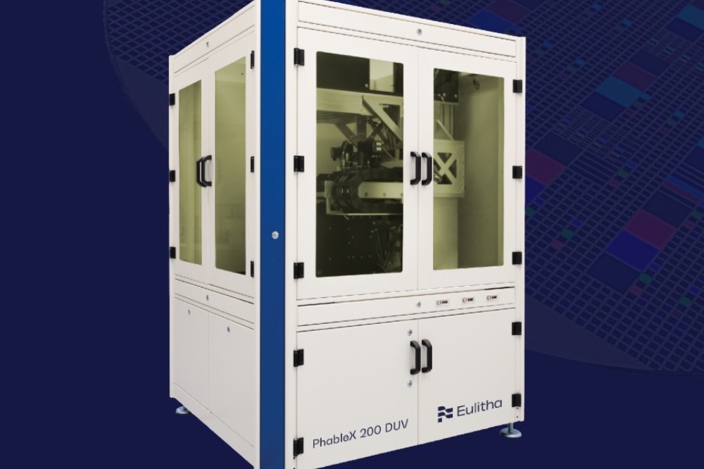
Eulitha’s tool platforms use proprietary non-contact optical lithography technology, known as displacement Talbot lithography (DTL), to deliver a range of advantages. High-resolution, precision patterning is ideal for advanced VCSEL arrays, while its large exposure field covers an entire 6-inch wafer in a single shot, reducing stitching errors and enhancing uniformity, according to the company.
After serving the DFB application market for many years, “VCSEL technology is evolving rapidly, and the market needs lithography tools that can keep up,” said Harun Solak, CEO of Eulitha. “Our PhableX systems are enabling our customers in Asia to scale up their 6-inch VCSEL production with confidence, delivering the precision and productivity needed to address growing demand in critical sectors like LiDAR and optical interconnects.”