Taking the guesswork out of SiC production
Thanks to advances in metrology, it’s now possible to scrutinise a SiC puck before it’s wafered and identify material defects that govern yield and profitability.
BY IVAN ORLOV, CAROLINE CHÈZE AND FRÉDÉRIC FALISE FROM SCIENTIFIC VISUAL, AND MARKUS STÖHR AND MICHAEL SCHÖLER FROM PVA TEPLA
Within the semiconductor industry, SiC is a transformative material. This wide bandgap compound drives innovation in power electronics, electric vehicles, renewable energy and advanced communications, thanks to its remarkable properties that include a high electron saturation velocity and breakdown field, exceptional thermal conductivity and mechanical robustness. These strengths enable diodes and transistors to operate at higher voltages, higher frequencies and more extreme temperatures than ever before.
We have been closely following the evolution of SiC and have witnessed staggering progress that’s been made over the last three decades to position this material as the backbone of efficient power electronics. We’re not alone in knowing there’s far more to come, with many forecasting SiC will remain central to the industry for the foreseeable future.
While today SiC is seen almost exclusively as a material for high-performance power devices, its potential extends to several other promising applications, including AR glasses, interposer layers in advanced packaging, data centers, and AI chips.
All these applications are leading to an increase in demand for high-quality substrates at accessible prices. There is plenty of headroom when it comes to improving the quality and, especially, the yield of SiC material. These improvements, however, are hindered by crystalline defects that impact device performance and reliability.
To name just a few examples, there are micropipes that threaten to trigger leakage currents and breakdown, basal plane dislocations and stacking faults that cause bipolar degradation, and polytype regions that may lead to premature failure.
To mitigate these risks, it is imperative to identify and reject ‘killer’ defects. However, today’s practice is to undertake comprehensive defect inspection at the wafer stage (see Figure 1) – and we would argue that’s too late, given that by then significant time and cost have already been invested in slicing and polishing.
It’s easy for downstream device makers and final users to overlook the significance of this problem, because defective material is filtered out earlier in the chain. Yet, the associated cost is built into every SiC device.
To fully understand the importance of this issue, note that substrates can represent up to 40 percent of the final device cost, and SiC material yields can be as low as 50 percent. Thus, continuing to only detect ‘killer’ defects at the wafer stage is a substantial cost barrier to mass adoption of SiC.
As SiC utilisation accelerates, our industry faces a pressing question: How can manufacturers ensure a high substrate quality while increasing wafer diameter? In response, PVA TePla and Scientific Visual now offer pioneering metrology solutions that redefine quality control for SiC.
The SiC Puck Scanner
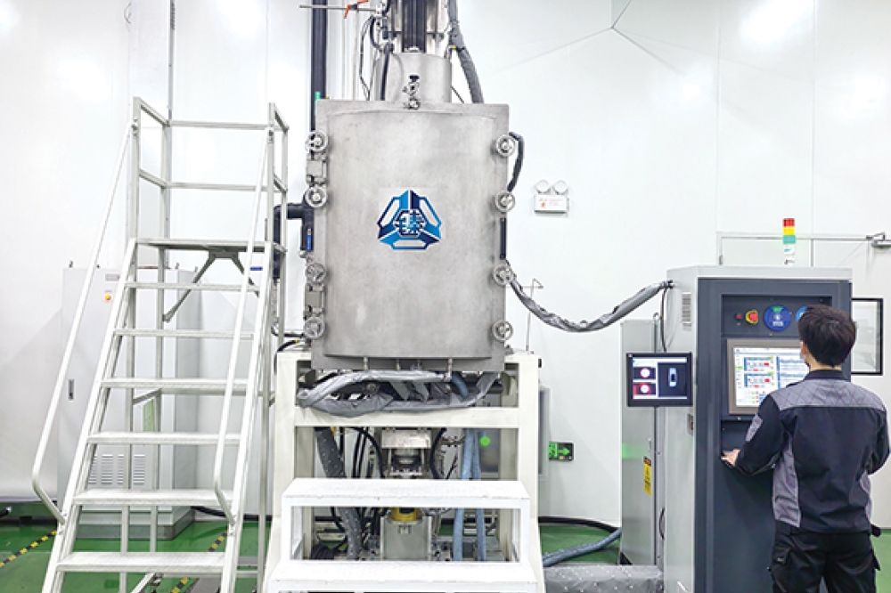
This September we unveiled the new SiC Puck Scanner at the International Conference on SiC and Related Materials, in Busan, South Korea. It is the first system to deliver non-destructive three-dimensional defect mapping directly within the puck volume (see Figure 2). It’s a game changer, leveraging advanced tomography to visualise critical defects before any wafering or costly processing begins.
With this tool, sub-standard pucks can be set aside prior to the costly wafering stage, allowing manufacturers to dedicate their slicing capacity solely to high-grade material. For the first time, producers can apply reproducible, quantitative defect metrics rather than relying on subjective visual checks.
A further advantage is that the scanner enables SiC substrate makers to move beyond ‘one-size- fits-all’ decisions and instead adopt more tailored wafering strategies.

Figure 1. Traditionally, the first comprehensive control of SiC defects in the production chain takes place at wafer level (red triangle), when substantial resources have already been devoted to processing. The new SiC Puck scanner shifts the quality control to an earlier stage (green triangle).
For instance, by drawing on precise defect coordinates, manufacturers can optimise wafering strategies by specifying the optimal cut levels. In case of wire-saw slicing, the goal is to position more defects within the kerf, thus excluding them from future wafers. This is achieved through Smart Wafering, a computer-aided patent-protected routine embedded in the YieldPro software that computes the most efficient puck position (offset) in a wafering system. As an example, we measured a 7 percent or greater increase in quality wafers compared to the ‘blind’ wafering in low- and mid-defective pucks.
In laser wafering, this technique allows one to identify suitable slicing regions and skip overly defective areas that could distort the cleaving track. Maximising yield is achieved by reducing processing, and delivering more high-quality material – all without expanding growing capacity. Additionally, each puck can be assigned to applications most aligned with its defect profile.

Figure 2. 3D defect map – output of the SiC Puck Scanner. Shown here is the puck that’s been used for the end-to-end study. Scans reveal lattice defects with micron-scale resolution, including polytypes, micropipes, voids, inclusions, dislocation clusters, and others. Colours correspond to defect morphology.
Volumetric defect mapping allows manufacturers to make data-driven decisions at the earliest possible point in the production chain. In practice, we have found that up to 50-60 percent of the wafering cost can be preserved by rejecting defective material early, rather than scrapping wafers after processing. Furthermore, digital maps provides transparent quality data that can be shared with colleagues and customers.
The benefits of puck scanning extend well beyond immediate cost savings. Scanning also serves as a tool for rapid improvement of bulk SiC growth. Each crystal defect is a message about a growth issue. Interpreting these messages promptly is key.
A traditional quality feedback loop involves puck wafering, wafer-level inspection, and a subsequent feeding of quality measurements back to the crystal growth team – a process that often takes months, with the message arriving too late to take corrective measures. The original wafer sequence in the puck is frequently lost, hindering efforts to trace the stack of defect formation in the puck. The puck scanning keeps the information and shortens the feedback loop to just a few hours. Now growth teams can inspect the furnace output almost instantly (grinding is still needed) and adjust parameters prior to starting the next growth cycle. For the first time, producers can quantitatively measure the effectiveness of recipe changes or furnace modifications on defect reduction. After all, what gets measured gets managed.
As well as driving yield improvements in traditional production, we are working to open new possibilities. Let’s now talk about the financial implications.
Down the production chain, the value of epi-ready wafers is graded by well-established metrics, that include defectiveness. Knowing the defect constellation while still at the puck stage makes it possible to predict these metrics in advance. This feature, currently in beta testing, is embedded within the YieldPro software coming with the new scanner. It lets users define custom wafer grades – such as Prime, Production, or Engineering – based on specific defect limits or existing industry standards. Using 3D puck scans, future wafers are auto-classified accordingly after the puck scanning. These grading protocols can be shared with downstream partners or customers.
This capability in turn allows manufacturers to evaluate puck processing profitability, factoring in defect levels, as well as wafering and polishing costs.
For example, the YieldPro software can build a profitability curve as a function of wafer thickness to assess how different wafer thicknesses influence financial gain (see Figure 3).

Figure 3. Profitability plot of a puck processing. It shows profit as a function of wafer thickness, taking into account defect distribution, as well as wafering and polishing costs. Coloured curves represent the number of wafers obtained in each grade, while the white curve indicates the total monetary profit. In this example, the maximum number of premium- grade wafers is achieved at a thickness of 0.3 mm.
As trade of pucks between growers and wafer manufacturers increases, objectively determining their yields is becoming increasingly important. Thanks to an assessment of quality at the puck level – before wafering begins – manufacturers of SiC substrates can align their production with specific orders, customer requirements, and market conditions.
Given the significant benefits of the SiC Puck Scanner, it’s not surprising that we are seeing swift interest in it. The upstream chain is now adopting automated quality control, following the trend established downstream.
Case Study: From puck to wafer – digital traceability in action
The SiC Puck Scanner can detect a wide range of defects: polytypes, micropipes, voids, inclusions, dislocation clusters, microcracks, and more. While the device is not a substitute for post-wafering inspection, as it’s possible that some minor defects may go undetected, it provides an essential first line of defence. During the scanner’s development, we continuously evaluated the accuracy of its performance by studying the correlation between puck inspection results and wafer-level defects through end-to-end case studies. While most of the tested material remains under NDAs, we received permission to disclose one case involving one of the thickest pucks we inspected.

Figure 4. Example of correlation between SiC puck inspection and wafer inspection (a) 1 mm-thick layer taken from the SiC Puck 3D twin at 1.62 mm depth, (b) the corresponding wafer under UV light, (c) the same wafer analysed by dislocation and stress mapping.
A 150 mm-diameter, 40.7 mm-thick SiC puck was scanned in SiC Puck Scanner to generate a full volumetric defect map. It was then sliced into 1 mm-thick wafers and analysed with traditional wafer inspection methods: Raman spectroscopy, UV illumination and near-infrared photoluminescence imaging. By tracing initial wafer orientations and positions within the puck, we were able to reconstruct detected defects layer by layer for the above techniques, and correlate them with the initial puck scan.
Results demonstrated a strong correlation between the defects detected in the puck and those observed in extracted wafers (see Figures 4 and 5). As expected, the characterisation revealed polytype regions, dislocation walls, and inclusions present in the sample – but not individual dislocations.
Finally, the produced wafers were inspected for stress using SIRD SiC 200 – Scanning InfraRed Depolarization stress-measurement technique (see below). This allows one to bring the volumetric defect results and post-wafering stress measurement into one 3D model (on the cover page), and study the correlation between internal defects and stress level in the material, which paves the way for multi-method metrology.
SiC-Wafer-Stress Metrology: The SIRD SiC 200 system
Stress measurements at the wafer level can be performed using new PVA TePla’s SIRD SiC 200 Scanning Infrared Depolarisation tool. This tool provides fully automated, quantitative stress mapping across a broad range of dopings and materials (see Figure 6). Because the entire measurement and evaluation process is recipe-based and features automated wafer handling, no operator intervention is required. This ensures reliability and repeatability at scale and supports 24/7 fab production. Achieving this level of automation is challenging; however, our team at PVA TePla draws on more than 25 years of experience in 300 mm silicon metrology.
Quantifying stress within a wafer is critical because stress correlates with defect growth and results in geometric deformations, such as bow and warpage. These deformations significantly reduce yield and impair device performance and reliability. By providing rapid, non-destructive, operator- independent stress analysis, the SIRD SiC 200 system enables customers to identify hidden risks before they escalate into costly problems. The SIRD SiC 200, having the ability to detect stresses at as low as 100 Pa, is therefore essential.

Figure 5. Example of correlation between SiC puck inspection and wafer inspection: (a) Raw image of 65 μm-thick layer at 1.62 mm depth revealed by the SiC Puck scanner, (b) Raman heat- map of part of the resulting wafer with thickness 1 mm.
High sensitivity in stress measurements is crucial because process control requires detecting minuscule changes in the stress field for effective and reliable monitoring of each step. Additionally, this sensitivity enables the detection of defects inside the wafer, from micropipes to threading dislocations. This is possible because each defect causes a characteristic surrounding stress field.
Measuring stress also offers valuable insight into process monitoring, from crystal growth to epitaxial-layer deposition. Each of these processes leaves a distinct stress fingerprint embedded within the wafer. This information becomes increasingly important as wafer sizes increase and process control windows narrow.
The SIRD SiC 200 system can be deployed in fabs to monitor the SiC substrate production process in its entirety – from measuring substrate-level stresses during crystal growth to detecting defects during epitaxy monitoring. After configuring a dedicated recipe for each process step, the system automatically measures and analyses wafers to calculate key indicators such as stress distribution and defect count. No operator access is necessary, because everything operates via SECS/GEM and overhead transport systems, in compliance with SEMI GEM300 standards.

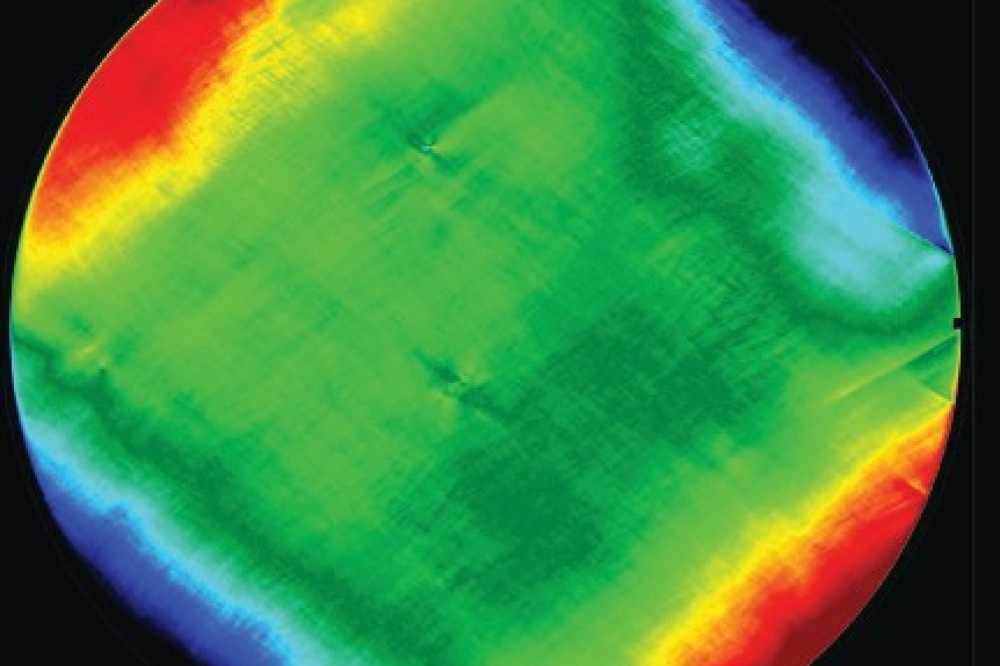
Figure 6. Shear stress map measured by the SIRD SiC 200 system. The map shows the shear stress distribution inside the 150 mm SiC wafer, with large, extended stress fields at the outer edge and smaller defect- induced stress fields.
Advanced metrology is set to revolutionise the SiC crystal industry as profoundly as it transformed the automotive and electronics manufacturing sectors earlier. Paradoxically, while the later stages of semiconductor production have embraced automated metrology, digital twins, and data-drivenquality feedback loops, the early stages – crystal growth, inspection, and wafering – still largely depend on intuition and manual judgment.
We are glad to witness a gradual shift in this landscape. At Scientific Visual and PVA TePla, we are helping shape that future, delivering innovations that provide measurable, real-world value. Early-stage defect detection, yield optimisation, and objective quality grading are no longer optional – they are essential for any company striving to compete in the SiC space.
With our solutions, manufacturers are empowered to reduce waste, boost throughput, and secure a clear competitive advantage. But adopting advanced metrology is about more than improving quality – it means forging a supply chain that is resilient, transparent, and ready for the future. Getting rid of unnecessary processing translates into a lesser environmental footprint of SiC substrate production. As the industry evolves, those who invest in early-stage inspection and digital traceability will stand best poised to lead not only in innovation but also in sustainability.
SiC’s future depends on intelligence and precision from the very start of the production chain. We are proud to be at the forefront of this development.
• We gratefully acknowledge the professional collaboration and timely support from Lapmaster Wolters (Switzerland, Germany) for puck wafering, Ntek Latent Technologies Inc. (Taiwan) for wafer surface preparation, VisionTec (Singapore) for wafer optical and photoluminescence characterisation, and the PVA TePla Tech‑Hub team (Germany) for Raman measurements.
• Ready to elevate your SiC production? Contact us for a demonstration or visit us at SEMICON Europa, Booth C1531.