High-bandwidth energy-efficient networks

Arrays of VCSELs promise to provide incredibly efficient LiFi communication at terabit data rates.
BY DENISE POWELL FROM THE COMPOUND SEMICONDUCTOR CENTRE, HOSSEIN SAFI FROM THE UNIVERSITY OF CAMBRIDGE, AND MOHAMED MISSOUS FROM INTEGRATED COMPOUND SEMICONDUCTORS
In a world that’s strongly focused on boosting energy generation to fulfil future demand, many overlook the benefits that come from trimming energy consumption. But those of us that are working within our community tend to know better, viewing device and material optimisation as levers with the potential to increase power conversion efficiency at the system level, and ultimately reduce the overall energy requirements from the grid.
It’s unlikely that you’ll be surprised by forecasts for a substantial increase in the energy consumption of data centres over the coming years. According to the International Energy Agency, in 2024 the global energy usage of data centres totalled around 415 TWh, equating to 1.5 percent of global consumption – and by 2030, demand is expected to have more than doubled to 945 TWh, primarily driven by AI-enabled data centres, for which energy demand is expected to quadruple. Ericsson has published related, additional insight in a whitepaper. That document includes a prediction that energy usage of digital services will continue to increase by 10 percent every year until 2030, by which time it will have climbed to reach approximately 1,100 TWh. To put these figures into perspective, in 2023 Scotland’s energy consumption totalled 64.5 TWh.
Growth of energy consumption at this rate is clearly unsustainable. It has led McKinsey to predict that there is going to be a data centre energy supply deficit of more than 15 GW in the US alone, due to demand for AI-ready capacity. And this view is not an outlier, with many online sources claiming that demand will outstrip supply, leading to electricity constraints in some areas. This is a problem that stretches far beyond Net Zero ideology; we simply do not have the energy-generation capability demanded by future architectures.
Unfortunately, energy is not the only problem facing the communications sector. Another issue is that the radio-frequency wireless networks are becoming increasingly congested, due to 4K video streaming, as well as a growing number of connected IoT devices – those in use are expected to reach 40 billion by 2030. In locations where there are a high number of connected devices in proximity, such as in a smart-city or smart-factory environments, the background noise level is higher, so stronger signals are needed from each device.
The congested RF network is very much a last mile problem. Today it’s not necessarily a significant challenge to deliver high-speed connectivity to a building, but it is becoming increasingly difficult to ensure a high-speed connection to every device on a specific network. And failing to do so is not an option, as AI-enabled Industry 4.0 solutions demand high-speed, uninterrupted connectivity of machines and devices.
If the AI revolution is to become a reality, there can be no delay in rolling out resilient indoor networks that combine low power consumption with high transmission speeds. Thankfully, compound semiconductor-based solutions can meet these requirements, addressing the ever-growing problems of increasing energy usage and the need for high bandwidth.
Figure 1. Addressable 5 x 5 VCSEL array.
Move over RF
The ideal solution has to tick quite a few boxes. It must be based on an architecture that: has a low energy consumption; delivers high bandwidth for ultra-capacity connectivity; is resilient, secure and scalable; and offers lower costs, for both ownership and operation.
Judged against this list, optical wireless communication (OWC) is a compelling candidate. Compared with RF solutions, this technology, using light to transfer data, offers a far broader spectrum for greater flexibility, immunity to interference, cost-efficiency and ease of deployment.
There’s both a strength and a weakness of OWC, associated with its line-of-sight communication. This characteristic makes it ultra-secure, with transmission confined, particularly in premises where access is restricted – but this can lead to problems in open spaces, as links can be disrupted or affected by environmental variations.
Note that when security is at a premium in indoor applications, OWC can easily be combined with additional security measures, such as quantum key distribution.
Within the OWC market, the fastest growing segment is Light Fidelity, often shortened to LiFi. Responsible for coining this term is the the University of Cambridge academic Harald Haas, who first demonstrated LiFi in a TED Talk in 2011, where he employed conventional LEDs for data transmission. In 2012 Haas co-founded pureLiFi, taking a Chief Scientific Officer role at this start-up, the first organisation to commercialise LiFi technology. The year after pureLiFi founded, it launched the Li-1st system, following an Innovate UK part-funded project with Cisco.
Latest generation of LiFi systems modulate infrared light in order to transmit data. This form of communication delivers far higher data rates than currently deployed WiFi systems, which have a practical data rate in the region of 1 Gbit s-1. Note that for indoor networks, one should avoid paying too much attention to published WiFi speeds, as they have little relevance, unless the router is used by one device at any one time. Anyone who has tested their home WiFi speed in frustration, using apps such as Speedtest, will unfortunately be familiar with the downsides of a shared bandwidth in a busy household.
Complimenting WiFi with LiFi could have extraordinary implications for future interactions with others, machines, devices and infrastructure.
Figure 2. VCSEL array mounted on a prototype package for characterisation.
Resilience through versatility
Whilst LEDs may appear to be an optimum choice for LiFi, allowing ordinary lighting infrastructure to double up as a transceiver (with some infrastructure modifications), the performance of these emitters is suboptimal, in terms of achievable bandwidth. In this regard lasers are far more attractive, with laser-based LiFi offering transmission speeds a hundred times faster.
Not all laser sources are well-suited to LiFi, or even OWC. Key criteria are a low-energy consumption, high bandwidth, ease of manufacture, reliability and scalability – and when judged against that list, there really is no match for the VCSEL.
Strengths of the VCSEL for deployment in the majority of OWC networks include high modulation speeds, good power-conversion efficiencies, ease of fabrication, and a significantly lower cost-of-manufacturing per die.
With edge-emitting and distributed-feedback lasers, output power scales linearly with die length and demands the support provided by more bulky subsystems that have a higher power consumption. These issues are avoided with VCSELs, thanks to vertical light emission out of the plane of the substrate. It is relatively easy to combine many VCSELs in arrays, enabling a hike in output power without a significant increase in die size.
Another attribute of the VCSEL is its Gaussian beam profile. This enables far-more-efficient links than those realised with LEDs, as a less powerful source provides the same transmitted power across the optical link.
Also featuring on the long list of impressive characteristics of the VCSEL is its tremendous flexibility, in terms of device architectures. Design engineers can consider single-mode devices through to stacked-junctions; the epitaxy and device options available are vast; and there’s also array scalability.
Figure 3. Schematic of the free-space link architecture developed at the University of Cambridge for data transmission
Certainly within REASON
Following the development of niche single-mode VCSELs for quantum clocks and magnetometers, UK partners Integrated Compound Semiconductors (ICS) in Manchester and the Compound Semiconductor Centre (CSC) in Cardiff joined forces with the LiFi team at Cambridge University, headed up by Haas under a future telecoms project.
Working together, we embarked on a two-year project called REASON: Realising Enabling Architectures and Solutions for Open Networks. Part-funded by the Department of Science Innovation and Technology – and benefitting from a total budget just shy of £12 million, as well as the involvement of UK-wide academic, RTO and industry heavy-weights – we have been focused on reshaping the future of open network architectures, with efforts directed towards openness and greater interoperability.
To put the scale of our activity into perspective, VCSEL development, coupled with novel modulation techniques, have been included as one of three strands under one of six work packages. Our focus in the work package was to develop custom device solutions for multiple-access networks, including advanced radio, optical-wireless and fibre technologies. The other two strands included GaN RF power amplifiers and InP optical amplifiers.
An attractive option for transmitting vast amounts data is spatial multiplexing. For this form of transmission, which is key to increasing aggregate data throughput, there’s a preference for individually addressable monolithic VCSEL array architectures. But this source brings challenges, in terms of both epitaxy and device fabrication. To ensure closely matched emitters, it is crucial to ensure uniform epitaxy and fabrication processes.
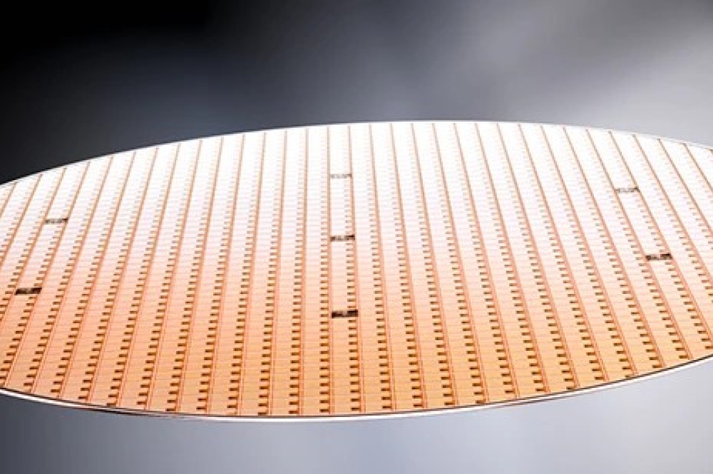
Through project REASON, we have developed small-scale, 5 x 5, addressable VCSEL arrays (see Figures 1 and 2). We began at 940 nm, before progressing to 980 nm and 1060 nm.
Building on quantum programmes, ICS designed epitaxial structures for three wavelength platforms and new device layouts, and also undertook array fabrication. CSC contributed high-uniformity epitaxy processes, crucial to formation of quantum devices and beneficial to array matching. The team at University of Cambridge set the specifications for the arrays, applied modulation techniques, and integrated beam-shaping to characterise VCSEL array performance in a custom OWC link.
Our best-performing devices were those emitting at 940 nm. These VCSELs met the per-element output power target of 5-10 mW at a drive current of 12-16 mA, with a threshold of 1.2 mW and a 10 GHz 3dB bandwidth. Notably, these devices were produced using established processes to demonstrate the feasibility of basic monolithic arrays for OWC. Their fabrication did not require significant optimisation of the epitaxy processes or device platform development. The variants at 1060 nm suffered from optical losses, due to a lack of full optimisation of the epitaxial process at this wavelength.
Using bespoke modulation and multiplexing techniques, the team at Cambridge University demonstrated record free-space aggregate data rates of over 300 Gbit s-1 for monolithic VCSEL arrays, at close to half the energy consumption of commercial WiFi systems. The results provide a promising platform for our collaboration to continue to develop and push the capability closer to 1200 nm for greater peak-powers.
The widely accepted eye-safe threshold for lasers is around 1400 nm. For wavelengths further into the infra-red, radiation is absorbed by the cornea without being focused on the retina.
According to theoretical research, the permissible peak-power for laser sources varies not only with wavelength, but also with beam waist, which can be controlled by adjusting the aperture width of the VCSEL. The maximum transmit power of the laser source increases linearly until around 1150 nm. Beyond that, the maximum transmit power increases exponentially until 1200 nm, before returning to a linear relationship.
The permissible peak-power curve, which depends on both wavelength and beam waist, equips system and device designers with significant flexibility in optimising system performance and cost, based on the application. For indoor applications, VCSEL arrays for LiFi ideally emit at wavelengths beyond 1200 nm. However, device and drive parameters can be tailored to ensure that the lasers are eye-safe at lower wavelengths.
Thanks to the versatility of VCSEL architectures, researchers can explore quite a few different opportunities. For example, one of the discrete single-mode 850 nm VCSELs developed during the QFoundry project to scale-up manufacturability of quantum photonic components has been characterised by the team at Bangor University in a 2.5 m OWC link. This effort involved a comparison with an off-the-shelf multimode VCSEL. The QFoundry VCSEL, fabricated by ICS using CSC epi, outperformed the off-the-shelf variant, boasting a lower relative intensity noise and twice the date rate – 38 Gbit s-1, compared with 19 Gbit s-1 for the multimode device – at an eye-safe transmitted optical power of around -1.47 dBm.
Based on our results, we are viewing VCSEL-based architectures as a possible pathway towards Tbit s-1 communications networks. There is a case to be made for VCSEL-based LiFi to support sustainable infrastructure for 6G and rapidly growing AI-enabled datacentres for a post-fibre paradigm, whilst addressing the increasing problem of congested RF networks.
Over the coming years, there will be an increase in demand for low-latency networks. They are fundamental to extended-reality immersive technologies that include augmented, virtual and mixed reality experiences, as well as holographic communication. VCSEL-based LiFi systems offering ultra-high bandwidths provide a pathway towards wide-scale adoption of multi-user setups, without impacting the user experience.
We expect the deployment and wider adoption of VCSEL-based LiFi communication networks to follow typical new technology adoption product lifecycles. There is still work to do at all levels of the supply chain, from epitaxy development through to device platform, package and system optimisation. Packaging technologies are going to have a big role to play in minimising parasitic capacitance, and VCSEL-based LiFi will require new customised package development.
Prototype devices are already offering a step-change in bandwidth versus power consumption. Thanks to this, when first-generation systems are available, they are likely to be adopted in applications at a higher margin, where bandwidth is absolutely critical. A subsequent generation of products will set to increase the bandwidth at the device level, as well as optimising modulation techniques.
Ultimately, whilst standards have embraced LiFi, there is still work to do in establishing appropriate business models, and interaction across infrastructure and network providers is needed to ensure that LiFi becomes a mainstream technology in commercial and residential environments.
CS can have the comms cake and eat it
Today, there is much debate over the value of Net Zero and AI. But the compound semiconductor community should welcome these revolutions with open arms.
What’s beyond doubt is that future networks will need to embrace a fusion of transmitter technologies, and the majority of them will involve compound semiconductors, including architectures based on GaAs, GaN and InP. And as these networks roll out, there’s a compelling case for reducing optical fibre usage and migrating to lower-power systems through efficient OWC networks. A shift in this direction has the potential to improve both the CapEx and the OpEx of the datacentres of tomorrow.
Low-cost VCSEL array-based OWC architectures, offering lower power consumption for the same output power, can also aid satellite networks that provide communication links. Deployment of these links is rising fast, and eye-safety is not a concern out in space, enabling greater flexibility in system and device design.
Recently, there has been a significant shift in the global political landscape, with more countries looking to have greater domestic capability surrounding the manufacture of key technologies. This upheaval brings an urgency for sovereign components in UK telecoms infrastructure that can offer resilience and enhanced security characteristics. Meeting this goal is not trivial, as historically there not been a high level of interaction across the communications supply chains. Our groundbreaking REASON project is helping to address this weakness by establishing collaboration across materials and device development, through to systems developers and network providers.
Our work forms part of our industry’s efforts in ensuring that compound semiconductors will capture every piece of the communications pie. Whether it’s long-distance or short-range links, or connected or wireless networks, III-V devices, including VCSELs for LiFi, are a key technology.


