
Researchers make novel low‑refresh energy gain cell memory
Researchers at Stanford University and TSMC have shown that adding an ultra-thin Al2O3 interlayer improves reliability and data retention in two-transistor gain cell memories (a kind of DRAM that offers a non-destructive read alterative to 6T SRAM).
The work is focused on oxide semiconductor FETs that use amorphous metal oxides — such as ITO and IGZO — for the active channel. 2T gain cell memories based on this technology are attractive for high-density on-chip storage, but retention and write margin are highly sensitive to the threshold voltage.
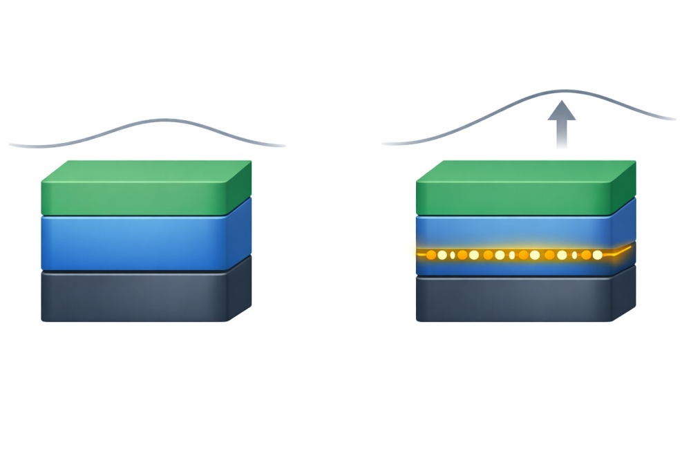
The team found that a sub 1nm Al2O3 layer creates an interface dipole that shifts the threshold voltage of oxide semiconductor FETs by up to 450–500 mV, while preserving mobility and drive current. This improves reliability and retention in 2T gain cell memories.
By enabling normal off operation without sacrificing on current, interface dipole threshold voltage tuning cuts leakage in the stored '1' state and can dramatically reduce refresh overhead, according to the team. Simulations calibrated to measurements indicate 50,000 times lower refresh energy compared with the baseline stack.
The key gain cell trade-off is that a too negative threshold voltage leads to storage node discharge (retention failure), while a too positive threshold voltage limits the charge written in the allotted write time (write failure).
Conventional threshold voltage shift methods, such as doping, thickness scaling, and anneals, often degrade mobility or subthreshold swing. The breakthrough here is importing a CMOSstyle interfacial dipole concept, but placing the dipole forming layer directly at the oxide semiconductor/high k interface using a low thermal budget 'dipole first' approach.
The team fabricated baseline devices with a hafnium oxide gate dielectric and dipoleengineered variants by inserting atomic layer deposited sub-1 nm Al2O3 layers at the interface to the oxide channel.
In tungsten-doped indium tungsten oxide FETs, the thickest dipole layer delivered the largest threshold voltage increase (450 mV), while statistics showed no systematic loss in on-current or field effect mobility. The threshold voltage offset persists from 85 °C down to cryogenic temperatures.
Reliability also improved: under worst case +2 V overdrive DC positive bias stress at 85 °C, interface dipole gain cells shifted by 60 mV versus 300 mV for the baseline. The approach generalises across other oxide channels (indium oxide, ITO, IGZO) and to short gate lengths (down to 50 nm).
The authors point to further reductions in stress induced threshold voltage drift via additional channel and stack optimisation (for example, stoichiometry tuning, fluorine doping, encapsulation) and to deeper mechanistic work to explain why different oxide channels show different dipole strength and saturation behaviour. A longer term goal is multi threshold voltage oxide integration for scaled gaincell arrays and gate all around oxide semiconductor transistors.
This work was recognised as a Technology Highlight at the 2025 Symposium on VLSI Technology and Circuits.
References
F. F. Athena et al., IEEE Transactions on Electron Devices, vol. 72, no. Dec. 2025.
F. F. Athena et al., 2025 Symposium on VLSI Technology and Circuits.


