
HEMTs: InAlGaN raises the ceiling
Thermal CVD equips next-generation InAlGaN/GaN HEMTs with high frequencies, exceptional powers and high reliability
BY ATSUSHI YAMADA FROM FUJITSU LIMITED
Extensively deployed in defence and communication systems, GaN-based semiconductors are held in high regard as optimal materials for high-power and high-frequency applications. However, due to decades of intense development, conventional AlGaN/GaN HEMTs are now encroaching the fundamental limits of this particular material system, making further improvements in output performance increasingly difficult. To overcome this plateau, innovative approaches are needed for next-generation device technologies that will sustain progress in advanced electronics.
A particularly promising candidate for raising the ceiling that limits what’s possible is a variant of the nitride-based HEMT that utilises indium-based nitride semiconductors in the barrier layer – it’s an alternative that is commonly referred to as the InAlGaN/GaN HEMT. Compared to its conventional cousin, the pairing of InAlGaN and GaN creates a two-dimensional electron gas (2DEG) with a higher density, an advantage that positions this material combination as a strong contender for next-generation devices optimised for the delivery of high powers.
Unfortunately, it not easy to unleash the full potential of InAlGaN materials. The issue is that this quaternary introduces a fundamental challenge, rooted in its chemical structure. There’s a relatively weak bond between indium and nitrogen that renders this class of material particularly vulnerable to damage during fabrication processes, especially those involving exposure to a plasma. Issues arising from the intrinsic fragility include the introduction of non-uniform surface potentials and a reduction in electron mobility – both adversely affect overall device performance.
One consequence of these drawbacks is that the InAlGaN/GaN HEMT is yet to demonstrate RF output characteristics that exceed those of the conventional AlGaN/GaN HEMT. It’s a state of affairs that highlights the ongoing need for innovation in epitaxial growth and process optimisation. Growth is held back by the adoption of epitaxial and process techniques originally developed for the traditional duo of AlGaN and GaN. Despite InAlGaN exhibiting distinct physical properties, conventional methods are employed without sufficient adaptation, obstructing this alloy from fully realising its potential.
To address this issue, our team at Fujitsu has undertaken a comprehensive re-evaluation of epitaxial growth conditions and process technologies, while focusing on the objective of developing device structures optimised for high-frequency, high-power operation. During this exercise, we directed our attention at the deposition conditions of the SiNx passivation layer, which plays a critical role in suppressing surface damage. Adopting this optimisation strategy enhanced electron mobility, and ultimately realised an output performance exceeding that of conventional AlGaN/GaN HEMTs.
Why InAlGaN?
The primary benefit of employing an InAlGaN barrier layer is not limited to simply attaining a high 2DEG density; rather, it is the simultaneous realisation of a high electron mobility and a high 2DEG density. One strength of InAlGaN is that it consistently exhibits a higher electron mobility than AlGaN at equivalent 2DEG densities, rendering it a compelling candidate for utilisation in next-generation devices (see Figure 1).

Figure 1. Dependence of the electron mobility on the 2DEG density in the InAlGaN/GaN and AlGaN/GaN HEMT.
In conventional AlGaN barriers, increasing the aluminium content enhances the 2DEG density, but at the expense of adding strain in the material. The downside of strain is an increase in the effective mass of the electrons, impairing their mobility and limiting device performance. Conversely, InAlGaN incorporates indium, a material that relaxes strain and boosts mobility, even at elevated 2DEG densities. This renders InAlGaN a well-optimised material system for maximising output power.
However, there are still drawbacks with InAlGaN barriers. While extremely high 2DEG densities are beneficial for increasing current, they can significantly reduce breakdown voltage, an essential parameter for high-power operation. Consequently, it is imperative for engineers to be meticulous in their material and device design, as this is critical to ensuring the optimal balance between 2DEG density and mobility.
In our work at Fujitsu, we excel in this regard, prioritising the enhancement of electron mobility as a key strategy for improving output power. By optimising the material structure and growth conditions, we have targeted the full exploitation of the intrinsic advantages of InAlGaN for high-performance HEMTs.
Optimising the epitaxial structure
Early research into InAlGaN-based HEMTs investigated the utilisation of the ternary InAlN as the barrier layer, because this alloy can be precisely lattice-matched to GaN at an indium composition of about 18 percent. Lattice-matched InAlN effectively suppresses crystal strain, and the substantial spontaneous polarisation difference between InAlN and GaN delivers a hike in the 2DEG density compared with that of conventional AlGaN/GaN HEMTs – it’s two-to-three times higher. Thanks to these combined strengths, InAlN/GaN structures are highly attractive for high-power applications.
However, there’s a price to pay for this lattice matching – a high indium content, which demands low-temperature growth. This compromise hampers thermal robustness and limits process compatibility, creating challenges for device reliability.
To tackle these issues, we have turned to the quaternary alloy InAlGaN. By fine-tuning the gallium, indium and aluminium content, we precisely control lattice parameters and polarisation characteristics. It’s possible to produce a heterostructure with the desired electrical properties while employing a reduced indium content that opens the door to elevated growth temperatures, key to enhancing thermal stability and reliability.
When adopting this approach, one must be mindful that InAlGaN is susceptible to significant alloy scattering, which threatens to degrade electron mobility. Crucial to mitigating this effect is the incorporation of a spacer layer. Often AlN is employed for this task. However, it’s hard to form a smooth AlN layer, due to the low thermal stability of underlying GaN, which complicates high-temperature growth. Another issue is that the growth of InAlGaN occurs at relatively low temperatures, hindering surface smoothing and even promoting roughness. Consequently, InAlGaN-based structures necessitate an even greater degree of surface flatness for AlN than conventional AlGaN/GaN HEMTs.
To address this challenge, we have undertaken a comprehensive optimisation of the growth rate, and an augmentation of ammonia supply. This has led to successful formation of a flat AlN spacer layer, and ultimately a higher electron mobility and an enhanced performance for the InAlGaN/GaN HEMTs.
Critical passivation
High-quality epitaxial layers are essential for enhancing the performance of InAlGaN-based HEMTs. However, it’s critical to not ignore the role played by the passivation layer – this must protect the device surface. One weakness of nitride semiconductors is their sensitivity to plasma processes, a vulnerability particularly pronounced in InAlGaN materials.
We address this issue with a thermal CVD method that eliminates plasma exposure during formation of the SiNx passivation layer. This approach has the objective of enhancing output power.
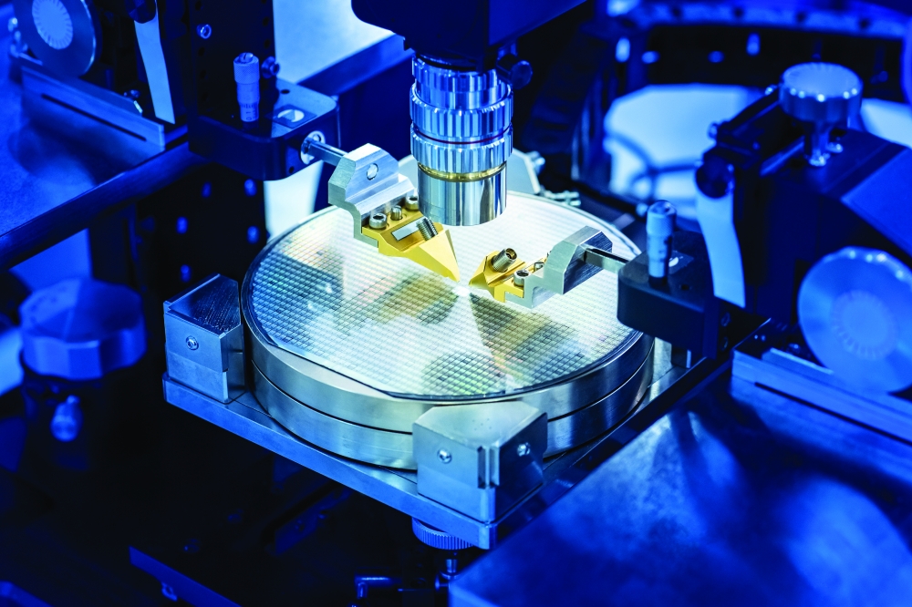
To produce our InAlGaN/GaN HEMTs we load substrates into a horizontal-flow MOCVD reactor and grow a heterostructure featuring a 6 nm-thick In0.05Al0.39Ga0.56N barrier layer and a 2 nm-thick AlN spacer. In this reactor, we then add a SiNx passivation layer by thermal CVD at 730 °C using silane and ammonia. To provide a comparative reference, we also produce a sample using plasma-enhanced CVD of SiNx at 250 °C – this is a form of passivation widely employed in the fabrication of AlGaN/GaN HEMTs.

Figure 2. Changes in (a) 2DEG density and (b) electron mobility before and after SiN passivation using thermal CVD and plasma-enhanced CVD techniques.
Electrical measurements reveal alterations to 2DEG density and electron mobility following SiNx deposition by thermal and plasma-enhanced CVD (see Figure 2). Both forms of CVD increase the 2DEG density. With thermal CVD, density of the 2DEG increases from 0.73 x 1013 cm-2 to 1.04 x 1013 cm-2; and with plasma-enhanced CVD, it increases it from 7.54 x 1012 cm-2 to 1.22 x 1013 cm-2. The extent of these changes is far smaller than that for electron mobility, which exhibits markedly divergent behaviour. Plasma-enhanced CVD induces a precipitous decline in mobility, falling from 2197 cm2 V-1 s-1 to 1290 cm2 V-1 s-1 – likely attributable to plasma-induced surface damage. In contrast, thermal CVD cause only a slight decrease in mobility – from 2198 cm2 V-1 s-1 to 2048 cm2 V-1 s-1 – indicating that the plasma-free process minimises surface damage and maintains uniformity. Taken together, the high electron mobility and the high 2DEG concentration realised by thermal CVD SiNx passivation yield a sheet resistance of just 293 Ω/sq. Another encouraging finding is that InAlGaN remains thermally stable, even at 730 °C.

Figure 3.Transfer characteristics of InAlGaN/GaN HEMTs with SiN passivation using thermal CVD and plasma-enhanced CVD techniques.
We have compared the transfer characteristics of our devices produced with different forms of CVD SiNx passivation (see Figure 3). Threshold voltages are similar: -0.69 V for thermal CVD, versus -0.86 V for plasma-enhanced CVD. The maximum transconductance of our HEMTs produced using thermal CVD, rather than plasma-enhanced CVD, is higher – 600 mS mm-1, compared with 504 mS mm-1 – and the maximum drain current is higher. We presume that this superiority is associated with a higher maximum drain current, due to a reduced on-resistance that results from enhanced mobility.
Another advantage of thermal CVD over its plasma-enhanced variant is that it provides a significant enhancement in breakdown performance, with the breakdown field increasing from 3.6 MV cm-1 to 5.9 MV cm-1. The three-terminal off-state breakdown voltage also increases, rising from 169 V to 227 V. These findings demonstrate the efficacy of thermal CVD SiNx passivation for enhancing the surface properties of InAlGaN/GaN HEMTs, and significantly improving their performance.

Figure 4. RF power characteristics of the InAlGaN/GaN HEMT with SiN passivation using thermal CVD and plasma-enhanced CVD techniques. Load-pull measurements were conducted at 8 GHz under pulsed operation, employing a pulse width of 10 µs and a duty cycle of 1 percent to mitigate the effects of self-heating. Measurements involved a bias current of 10 mA mm-1 and a total gate width of 1 mm.
Outstanding RF output
As one would expect, the benefits of thermal CVD are also observed in the RF output characteristics of InAlGaN/GaN HEMTs. Measurements at 8 GHz show that switching from plasma-enhanced CVD to thermal CVD delivers a significant increase in output power and power-added efficiency (see Figure 4). At a drain voltage of 60 V, the device with thermal CVD SiNx passivation realises a peak power-added efficiency of 53.9 percent, a linear gain of 12.1 dB, and a peak output power of 43.49 dBm. It is noteworthy that this device also supports high-voltage operation up to 90 V, significantly higher than the 60 V limit observed in the sample produced by plasma-enhanced CVD. As the drain-source voltage increases, the RF saturated output power density climbs steadily, ultimately attaining a power-added efficiency of 52.6 percent, a linear gain of 12.7 dB, and an output power of 44.91 dBm. This corresponds to an impressive power density of 31.0 W mm-1, among the highest reported values for this category of device.
For practical devices, a strong performance must by accompanied by reliability. Judged on this font, our HEMTs excel, with thermal-CVD-based SiNx passivation providing a substantial enhancement in device reliability. Early-stage tests have determined that InAlGaN/GaN HEMTs produced with plasma-enhanced CVD SiNx fail at a junction temperature of 307 °C. In sharp contrast, devices protected with thermal-CVD SiNx passivation demonstrate stable operation for over 900 hours under identical conditions. These findings indicate that InAlGaN/GaN HEMTs, produced using optimised thermal CVD SiNx passivation, exceed conventional AlGaN/GaN devices in both performance and reliability, making them compelling candidates for broad commercial adoption and long-term implementation in demanding applications.

Figure 5. Benchmark of the RF saturated output power densities (Psat) versus the drain-source voltage (Vds) of GaN-based HEMTs in the X-band.
Moving forward, we will continue to refine our InAlGaN/GaN HEMT technology, which will be essential in meeting the demands of next-generation power and communication systems. These efforts will include further research into thermal stability and reliability under extreme conditions, work that will help accelerate commercial adoption of these devices. As our fabrication techniques continue to evolve, the potential for InAlGaN to redefine high-frequency electronics is becoming increasingly tangible.
Further reading
A. Yamada et al. “Electron mobility
enhancement in metalorganic-vapor-phase-epitaxy-grown InAlN
high-electron-mobility transistors by control of surface morphology of spacer
layer,” Jpn. J. Appl. Phys. 57 01AD01 (2018).
A. Yamada et al. “31 W/mm at 8 GHz in InAlGaN/GaN HEMT With Thermal CVD SiNx Passivation,” IEEE Electron Device Lett. 45 324 (2024).


