A universal solution for chip heating

More powerful, more reliable devices may be realised by replacing substrates with a composite providing an exceptionally low thermal resistance.
BY RICHARD STEVENSON, EDITOR, CS MAGAZINE
At times, our industry appears a disparate entity. The high-power GaAs lasers diodes that cut and weld metals operate in a different sphere from their InP cousins that underpin the internet – and both of these emitters occupy different domains from the RF devices deployed in defence, and the wide bandgap diodes and transistors that are improving the efficiency of power delivery.
But there are common threads running through these various classes of compound semiconductor devices. One is that they are united by epitaxial growth, with gains on this front having far-reaching ramifications. And another, of high importance but not discussed as much, is that the performance of all these devices derives substantial benefits from better thermal management. Gains include higher output powers, greater efficiencies, and longer lifetimes.
A new, exciting and universal solution to this critical thermal management issue is now being pioneered by Dutch start-up CoolSem. It has just secured a pre-seed financing round that will support the commercialisation of its chip-cooling technology, involving removal of a substrate, which is replaced by a composite structure with a vastly superior thermal conductivity.
The trailblazer of this technology is CoolSem CEO and CTO, André van Geelen. Back in the early 1990s, during his time as a PhD student at Radboud University, he developed a key element of the start-up’s core technology – wafer-scale removal of a substrate from its epilayers via epitaxial lift-off, a proven process already in use for the formation of large, flexible III-V solar cells.
Since then, van Geelen has spent his entire career within the semiconductor industry, initially working for a number of high-profile companies – Philips, JDSU, ThreeFive Photonics, and NXP – where he gained insight into the issues associated with device heating, and how this limits performance.
For the last 10 years, most of his time has been devoted to consulting start-ups and working on the board of UK start-up Forefront RF. But recently he has also been mulling over his idea for superior thermal chip management, with his entrepreneurial side nagging away and eventually getting the better of him: “This is how I started last year. Basically, I stopped most of my consultancy and went for it.”
A classy composite
There are essentially two parts to the CoolSem technology, which provides a more elegant solution to chip heating than existing approaches based on attaching a cooler to either the chip or the package. Substrate removal is the first step, followed by the addition of a heat-sinking composite.
For III-V structures, substrates may be removed and re-used by epitaxial lift-off, a process that involves the etching of a sacrificial layer. That’s not an option for devices grown on silicon, but in this case grinding-and-polishing approach is available, a technique widely used on 200 mm and 300 mm wafers.
To determine the composition of the composite that delivers the best results, van Geelen has undertaken one- and two-dimensional simulations of various material combinations, considering mechanical and thermomechanical stresses.
“One of our customers actually put the key parameters that we provided in their device and found a clear improvement. In this case, this was on a power amplifier for Satcom.”
This verification of CoolSem’s technology underscores the potential of the proprietary composite, which features a wide bandgap material beside the chip, a central compliance layer and a base metal. This trio, referred to as WaLTIS – that’s short for Wafer-Level Thermal Interface Stack – has a thermal-resistance-per-mm2 of just 0.2 K W-1. That’s far lower than a typical device with a Au/Sn solder, which would have a value of 3 K W-1. Thanks to the thermal superiority, chips run at far lower operating temperatures, with differences between the device and its foundation falling from between 30°C and 60°C to just 4°C.
As well as tremendous thermal properties, WaLTIS provides excellent mechanical support and avoids RF losses, crucial when used with power amplifiers.
One of the strengths of this technology is the generality of the solution, as WaLTIS is compatible with all semiconductor materials. The only change that might be applied from one device to another is the thickness of the compliance layer: “If you have extremely large die, you can imagine that the stresses in the stack become larger, so we need a little bit more compliance there,” says van Geelen.
To take his idea from the drawing board to commercial success, he has hand-picked three co-founders, all known to him from previous projects. They are: Commercial Officer Pieter Heersink, who van Geelen worked with on a previous start-up; Strategic Officer Robbert van der Waal, a co-worker at NXP; and Operational Officer Kees Steenbergen, a colleague at ThreeFive Photonics.
Following the coming together of these four in autumn 2025, the team has expanded with the addition of four engineers, plus two-to-three external contributors. Together they are supported by an undisclosed level of funding: roughly half of this is equity; one-quarter loans; and the other quarter a grant from the Dutch Future Network Services Programme, which focuses on future RF technologies.

The founder of CoolSem are: CEO and CTO André van Geelen (front right), Operational Officer Kees Steenbergen (front left), Commercial Officer Pieter Heersink (back left), and Strategic Officer Robbert van der Waal (back left).
A hands-on approach
CoolSem’s business plan is to provide a ‘mid-end’ foundry service. This involves receiving processed epiwafers, followed by the application of CoolSem technology and the dispatching chips on a plastic thin-film backing to packaging houses.
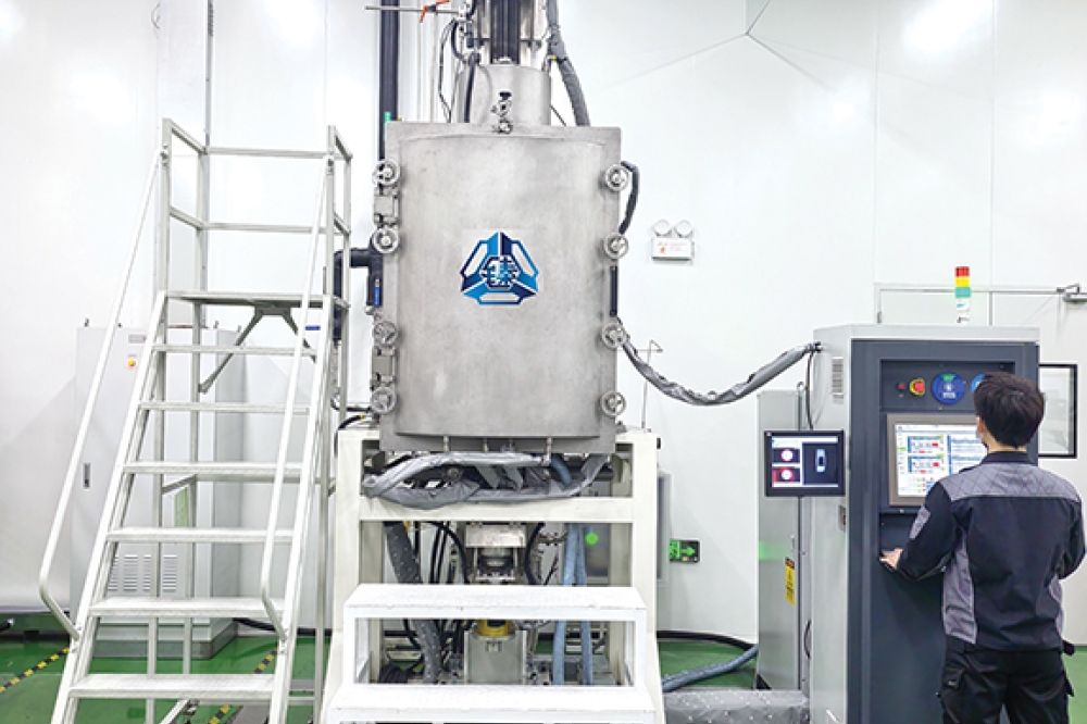
To begin with, CoolSem will carry out its processes with local external partners, based in The Netherlands and Germany. “Some provide facilities as well. It's not just services,” says van Geelen, who reveals that these relationships have provided CoolSem with access to a cleanroom, which can be used for prototyping and initial engineering.
Looking further ahead, CoolSem plans to carry out its processes in-house. Accomplishing this only requires a few tools, an investment totalling €5-10 million.
One of the benefits of this is that it will help CoolSem advance its technology. And in addition, it will reduce the risk that potential customers will take.
“We plan to bring up to pilot volumes, which could be 30,000 wafers a year. Anything beyond that, I think most customers we're working with would feel quite comfortable bringing that over to their own environment,” says van Geelen, explaining that this transition involves a licensing model.
If makers of VCSELs and other forms of laser adopt CoolSem’s technology, it could have a big impact – van Geelen suggests increases in efficiency from around 25 percent to twice that. Substantial gains are also possible in RF devices. In power devices, increases in efficiency are more modest, but given emphasis on minimising electrical consumption, such savings will still have much value.
To transition CoolSem’s technology from promise to reality, the aim is to demonstrate its capabilities to customers this summer. “That's also the point where we will engage with two or three customers, to demonstrate the technology in their applications.”
The hope is that success with the later will occur in summer 2027, paving the way for new generations of chips that run cooler, while performing better.