
Real-time view reveals 2D semi growth secrets
2D semiconductors have emerged as promising candidates for future electronics due to their unique properties. However, despite intense research interest, controlling the growth of high-quality 2D semiconductor crystals has remained a major scientific and technological challenge.
Now, a research team led by Hiroo Suzuki from the Department of Electrical and Communication Engineering at Okayama University, Japan, together with Kaoru Hisama from Shinshu University and Shun Fujii from Keio University, has overcome a key barrier by directly observing how 2D semiconductors grow at the atomic scale.
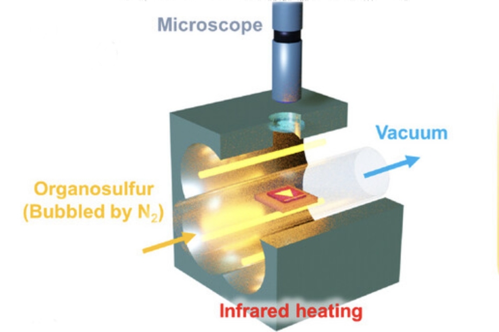
Using an advanced in situ observation system, the researchers captured real-time images of monolayer transition metal dichalcogenides (TMDCs) forming inside a micro-confined reaction space.
The study 'Inside the Microreactor: In Situ Real-Time Observation of Vapor–Liquid–Solid Growth of Monolayer TMDCs' was published on December 12, 2025, in the journal Advanced Science.
The work builds on earlier success by the team in synthesising large-area monolayer TMDC single crystals using a substrate-stacked microreactor. While that method consistently produced high-quality materials, the mechanisms governing crystal growth inside the confined space were poorly understood.
“We could make excellent crystals, but we did not know exactly how they were forming,” said Suzuki. “Without that understanding, it is difficult to reliably design materials for specific device applications.”
To address this gap, the researchers developed an infrared-heated CVD system that allowed them to observe crystal growth as it happened. By carefully tuning precursor concentration and sulphur supply, they identified multiple growth regimes with distinct crystal shapes and behaviours.
Under some conditions, conventional triangular crystals formed. Under others, large hexagonal crystals rapidly expanded with molten precursor droplets accumulating along their edges. In sulphur-rich environments, ribbon-like crystals emerged, bending and changing direction in response to atomic-scale features of the substrate.
One of the most striking observations was the dynamic behavior of molten precursor droplets. The team found that sulphur incorporation lowered the melting point and surface tension of the precursor, increasing droplet mobility.
These droplets migrated across the substrate via surface tension gradients, known as the Marangoni effect, continuously feeding material into the growing crystal. “Watching the droplets move and directly contribute to crystal growth was a turning point,” Hisama explained. “It allowed us to confirm growth mechanisms that had previously only been inferred.”
By revealing how crystal shape and quality depend on growth conditions, the study provides a practical framework for engineering 2D semiconductors with unprecedented precision. This control is essential for overcoming current limitations in semiconductor integrated circuits, which are struggling to achieve further miniaturization and energy efficiency using silicon alone.
The implications extend beyond conventional electronics, say the researchers. Precisely engineered 2D semiconductors could lead to faster and more power-efficient smartphones, flexible and wearable sensors, and compact local power generation devices.
In the longer term, the findings may support the development of highly integrated, low-energy semiconductor platforms for artificial intelligence and Internet of Everything systems, including advanced monitoring technologies in healthcare and welfare sectors.
Suzuki emphasised the significance of the study and said: “This research shows that direct observation is the key to true materials control. By understanding how 2-dimensional semiconductors grow, we can design the next generation of electronic devices from the atomic level upward.”
Pictured above: Schematic of the in situ observation CVD system. Infrared heating furnace equipped with an optical window for observing the inside of the chamber using an optical microscope.


