
News Article
Agilent advances modelling for GaN HEMTs
The technology can also be applied to nanoscale 3D FinFETs
Agilent Technologies has developed several innovations for the 2014 release of its suite of device modelling and characterisation software tools.
The suite comprises Agilent EEsof EDA's Integrated Circuits Characterisation and Analysis Program (IC-CAP), Model Builder Program (MBP), and Model Quality Assurance (MQA).
"Over the past few years, we've steadily expanded our device modeling platform through internal development and acquisition of key technologies," says Brian Chen, Agilent's device modelling planning manager. "This marks the first release of our entire portfolio and represents a significant advancement toward our vision of being a partner that uniquely delivers a complete end-to-end, measurement-to-modelling solution."
Advanced Modelling Capabilities
The new software release features three advanced device modeling packages for Agilent's DynaFET, BSIM6, and BSIM-CMG models.
BSIM6 is a model for bulk MOSFETs, offering important improvements for analog/RF applications over its predecessor, BSIM4. BSIM-CMG is the industry-standard model for sub-20 nm 3-D FinFET technologies. Modelling solutions for both BSIM6 and BSIM-CMG in the 2014 release are designed to help the semiconductor industry understand and use these new technologies.
The DynaFET modelling package is based on internally developed technology and is an integral part of Agilent's GaN HEMT characterisation, modelling and simulation solution. The GaN HEMT modelling package provides a GUI-based turnkey solution for DynaFET model generation.
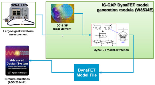
Using artificial neural networks for charge and current formulations, and incorporating trapping/de-trapping and self-heating effects, the time-domain DynaFET model is capable of fitting accurately to DC, linear and large-signal measurement data-all simultaneously.
This allows a single model file to be used for the design of different applications under various bias conditions, all with accurate simulation results.
Additional Enhancements
The 2014 device modelling and characterisation software release also provides a number of new and enhanced features designed to noticeably improve productivity across the end-to-end work flow of device characterisation, model generation and model validation.
These enhancements include a programming editor, faster simulation speed with major simulators, expanded mismatch and variation modelling solutions.
Also, there is a streamlined and flexible user interface to create, manage, monitor, and debug measurement test plans.
U.S. Pricing and Availability
Agilent's 2014 device modelling and characterisation software release will be available in July.
In addition, on September 19th, 2013, Agilent announced plans to separate into two publicly traded companies through a tax-free spinoff of its electronic measurement business. The new company is named Keysight Technologies, Inc. The separation is expected to be completed in early November 2014.
The suite comprises Agilent EEsof EDA's Integrated Circuits Characterisation and Analysis Program (IC-CAP), Model Builder Program (MBP), and Model Quality Assurance (MQA).
"Over the past few years, we've steadily expanded our device modeling platform through internal development and acquisition of key technologies," says Brian Chen, Agilent's device modelling planning manager. "This marks the first release of our entire portfolio and represents a significant advancement toward our vision of being a partner that uniquely delivers a complete end-to-end, measurement-to-modelling solution."
Advanced Modelling Capabilities
The new software release features three advanced device modeling packages for Agilent's DynaFET, BSIM6, and BSIM-CMG models.
BSIM6 is a model for bulk MOSFETs, offering important improvements for analog/RF applications over its predecessor, BSIM4. BSIM-CMG is the industry-standard model for sub-20 nm 3-D FinFET technologies. Modelling solutions for both BSIM6 and BSIM-CMG in the 2014 release are designed to help the semiconductor industry understand and use these new technologies.
The DynaFET modelling package is based on internally developed technology and is an integral part of Agilent's GaN HEMT characterisation, modelling and simulation solution. The GaN HEMT modelling package provides a GUI-based turnkey solution for DynaFET model generation.
Using artificial neural networks for charge and current formulations, and incorporating trapping/de-trapping and self-heating effects, the time-domain DynaFET model is capable of fitting accurately to DC, linear and large-signal measurement data-all simultaneously.
This allows a single model file to be used for the design of different applications under various bias conditions, all with accurate simulation results.
Additional Enhancements
The 2014 device modelling and characterisation software release also provides a number of new and enhanced features designed to noticeably improve productivity across the end-to-end work flow of device characterisation, model generation and model validation.
These enhancements include a programming editor, faster simulation speed with major simulators, expanded mismatch and variation modelling solutions.
Also, there is a streamlined and flexible user interface to create, manage, monitor, and debug measurement test plans.
U.S. Pricing and Availability
Agilent's 2014 device modelling and characterisation software release will be available in July.
In addition, on September 19th, 2013, Agilent announced plans to separate into two publicly traded companies through a tax-free spinoff of its electronic measurement business. The new company is named Keysight Technologies, Inc. The separation is expected to be completed in early November 2014.


