
Keeping LEDs cool
Claiming breakthrough performance with its metal-clad PCB substrates, Nanotherm, has already made inroads into LED markets, reports Compound Semiconductor.
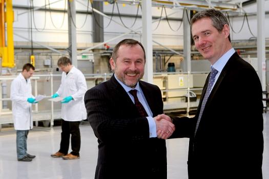
Dr Pavel Shashkov, CTO (left) and Ralph Weir, CEO: Nanotherm is rolling out its heat dissipation materials in high volumes to meet the growing needs of LED makers. [Nanotherm]
As the LED industry shifts to ever-higher brightness LEDs, the race is on to develop better thermal management strategies to dissipate heat. During LED operation a hefty 75% of applied electrical power is converted to waste heat, and be it by heatsink, heatpipe or cooling fan, how this heat is removed drastically affects LED performance and lifetime.
UK-based start-up, Nanotherm, claims to have the answer. Founded in 2010 by Pavel Shashkov and Segey Usov, former researchers at the Moscow State University, the company has developed a range of novel aluminium PCB substrates to act as heatsinks for electronics devices.
Currently targeting high performance LED markets, the substrates comprise an aluminium sheet, in which the surface - the top 10 to 30 microns - has been electrochemically converted to an alumina dielectric layer. A layer of copper is then epoxy-bonded or deposited to the dielectric layer, depending on customer budget, creating a circuit layer on the sheet, ready for PCB processing on industry-standard lines.
Shashkov and Usov claim their alumina dielectric layer provides excellent isolation with much improved thermal performance over the standard epoxies used as conventional dielectrics. The alumina layer is also up to ten times thinner than conventional epoxy layers and boasts a bulk thermal conductivity of 7 W m-1 K-1 whereas high thermal conductivity epoxies come in at some 3 W m-1 K-1.
And pleasingly for Nanotherm, its independent tests indicate the thermal resistance of the overall PCB substrates is 20% less than today's metal-backed PCBs, reducing LED operating temperatures by as much as 20ºC. As recently-appointed chief executive, Ralph Weir puts it: "I think this is a product that when engineers see it they say 'wow, I really love that'."
Patented process
The key to success is the conversion of the metal surface to an extremely thin dielectric layer. This process has roots in so-called plasma electrolytic oxidation (PEO), an electrochemical process similar to anodising, and developed by Shashkov and Usov more than a decade ago, to harden metal alloys for engineering applications.
Like anodisation, metal alloys, such as magnesium and aluminium, are dipped into a liquid electrolyte with an electric potential than applied to form an oxide-based ceramic - magnesia and alumina - at the alloy surface. However, PEO employs higher potentials so voltage discharges occur with the resulting plasma modifying the structure of the oxide layer. For example, sequences of voltage pulses can alter the surface roughness and porosity of the coating to produce harder-wearing surfaces.
Shashkov and Usov spent the best part of the 1990s developing the hardness treatment, setting up Cambridge-based Keronite, in 2000, to exploit the technology. But while the treatment produces a hard-wearing, as well as thermally conductive and electrically insulating surface layer, porosity within this layer renders the treatment useless for electronic applications.
With this in mind, the pair went on to develop a new process that delivers an oxide ceramic surface layer comprising very densely-packed crystals with a lot less porosity, and launched Nanotherm in 2010. Details on how the surface layer is formed are scant although patent searches reveal a colloidal alkaline electrolyte is likely used, containing ceramic particles less than 100 nm in diameter.
Meanwhile, the electrical treatment comprises a sequence of positive and negative voltage pulses to minimise micro-discharges during coat formation and better control porosity and surface roughness.
When asked about the process, Weir quips: "I wouldn't like to have to kill you", but confirms: "It is a heavily patented process, but the key is what's now in the electrolyte and the way the electrical power is applied; an enormous amount of control goes into this."

With a thin dielectric layer, Nanotherm materials have a short thermal path from the source "“ a semiconductor device soldered to the copper surface "“ to the heatsink. [Nanotherm]
But while heavily under wraps, industry players have proven keen to trial the process. In response to supplier demand, the company recently set up its first production line in Cambridge, which according to Weir is 'ramping up nicely'. And plans are now underway to have two more lines up and running by mid-2015.
"We're already supplying to quite a number of people with a lot of our production going out to PCB processing companies that are then taking it out to the LED market," adds Weir.
For example, Nanotherm has forged a partnership with Scotland-based electronics packaging player, Optocap, already shipping orders to LED customers. And the company has also joined forces with PCB manufacturer, Spirit Circuits, UK, again to supply substrates to LED markets
Weir won't provide specifics on price, simply saying, 'we talk about being a Ferrari for the price of a Ford', but as he asserts: "Our partners say our substrates outperform any other aluminium boards by 25 to 35%."
"Also thermal PCB copper boards exist that are heavier and much more expensive than our substrates yet we can outperform these by 2 to 3%," he adds.
So where next for the UK-based start-up? According to Weir, while the company's next production line will service the LED industry, the company is also eyeing power electronics markets. "The reality is the lines can produce materials for either markets," he says.
What's more, the company is also developing substrates to rival high performance aluminium nitride ceramic tiles. As Weir explains, during fabrication of the company's 'entry-level' boards, a layer of copper is bonded to the dielectric layer using a four micron epoxy adhesive to create the circuit layer. But the company is also using thin film deposition techniques to directly apply the copper circuit layer, producing a metal-backed PCB with performance to rival that of AlN tiles but at a lower cost.
"Partnerships with existing suppliers in the LED and power electronics packaging markets are key to us... and we will now scale the business up through such partnerships," he says. "We've got the production facilities to be a world player, so now it's all about that big scale up to reach the big volumes."


