
POET to work with Third Party Foundry
Plans include shrinking 100nm process to 40nm
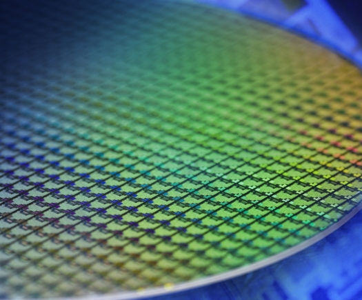
POET Technologies, developer of the planar opto-electronic technology (POET) platform for making chips with both electronic and optical elements on a single wafer, has announced an agreement with a "˜3rd party foundry' to reproduce and enhance repeatability of the 100nm scale results obtained at the company's labs located at the University of Connecticut (UCONN). The '3rd party foundry' will also assist the POET team in shrinking the 100nm PET devices and process to a 40nm feature size.
Definition and repeatability of 100nm has been difficult in the POET labs due to the limitations of available lithography tools and other equipment. The collaboration gives the POET team access to superior capability and diagnostics, allowing the POET approach to start to scale to both 3 in and 6 in wafers with much larger device count and across wafer alignment. The fine features will then be merged with optical lithography and other procedures necessary to transition to a manufacturing environment. In addition, the effort will target line width reductions from 100nm down to 40nm which should enable POET performance parameters to compete with present state-of-the-art processes. The reduction will be parallel to our efforts with our Synopsys TCAD collaboration.
Geoff Taylor, chief scientist and board member noted: "Developing the 100nm feature size technology in the current POET labs has proven to be challenging. With the collaboration of our '3rd party foundry;, we now have access to state of the art equipment highlighted by a state of the art ebeam writing tool. This will help us make the process more stable and predictable and help prove our process in a true manufacturing environment."
This announcement follows another regarding collaboration with Synopsys and the creation of the company's first Process Design Kit (PDK). This collaboration will see the development of an advanced model of the Company's PET devices targeting a technology node of 40nm, a significant production node of highly integrated systems-on-chip silicon CMOS device. The results of the physical devices at 40nm developed at the 3rd party foundry can then be correlated to the models of the PET technology developed using TCAD tools from Synopsys and vice-versa.
Peter Copetti, executive chairman Interim CEO concluded: "We now believe we have the right collaboration in place with Synopsys and our '3rd party foundry' to model our technology down to 40-nm and correlate our process to real physical device measurements. This should provide us with results needed to showcase our technology to potential customers at the optimum node for our platform. We expect synergistic benefits from having parallel operations with the same end target."


