Growing the Terahertz transistor

Breakthrough GaN-on-graphene growth brings Naval Research Laboratories researchers close to hot electron transistors. Compound Semiconductor reports.
Can NRL's low temperature atomic layer epitaxy help researchers grow GaN-on graphene structures for terahertz frequency applications?
Claiming a world first, researchers from the US-based Naval Research Laboratories have successfully grown a high-quality GaN film on graphene, a critical step to developing so-called hot electron transistors for terahertz frequency applications.
Using MOCVD, GaN films were grown on functionalised epitaxial graphene, over an AlN nucleation layer, yielding a crystalline quality on par with GaN grown on sapphire. What's more, lead researcher, Charles Eddy from NRL's Electronics Science and Technology division, says his team can use the same process to grow structures across a four inch wafer, setting the scene for cost-effective device manufacture.
Hot electron transistors (HETs) hold great promise for high-frequency, high-speed current switching applications as during operation, the electrons tunnel ballistically through base and collector structures. However, today's state-of-the-art HETs include a metal or heavily doped semiconductor base layer that impedes electron movement, limiting device performance.
With this in mind, researchers worldwide are turning to graphene as an alternative base layer material. Electrons fly though this so-called wonder material, enabling cut-off frequencies in excess of 1 THz, and pleasingly, researchers have mastered methods to grow a single layer of graphene - epitaxial graphene - on SiC substrates.
But while graphene solves a lot of problems, it also raises new issues. As Eddy puts it: "Graphene, and any other 2D material, has very good in-plane bonds, but not very good out-of-plane bonds. There aren't actually any atomic bonds to connect to if you want to try and grow a material, such as GaN, directly onto a graphene surface."
Indeed, deposit GaN directly onto a graphene surface and individual crystallites form instead of a continous film. And while researchers have modified the surface to circumvent this problem - treatments include plasma-spraying the surface and adding nanostructures - the resulting graphene-GaN interface can inhibit final device performance.
![]()
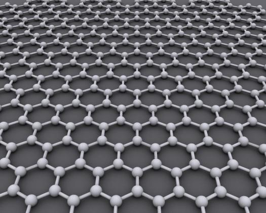
Terahertz designs: the NRL research team is pioneering GaN-on-graphene growth in a bid to fabricate hot electron transistors.
However, a surface modification process, originally pioneered by Eddy's team to integrate high K gate dielectrics with graphene, looks set to solve the problem. So-called fluorine functionalisation involves dosing the graphene surface with xenon difluoride to create semi-ionic carbon-fluorine bonds that provide nucleation sites for III-nitride deposition.
With the nucleation sites in place, Eddy and colleagues then deposit a buffer AlN film onto the functionalised graphene, prior to GaN growth. Aluminium atoms have a higher sticking coefficient than gallium atoms, and in Eddy's words: "'Gallium just isn't as easy to stick as aluminium."
But the surface modification success comes with a hitch. The semi-ionic fluorine bonds can attach to the graphene surface while preserving its structure, but these bonds cannot withstand the high temperatures of conventional MOCVD.
"Ionic bonds would break the bonding in graphene and kill its electronic properties," says Eddy. "However, the [semi-ionic] bonds are very temperature sensitive, so to grow III-nitrides on graphene we really need a low temperature epitaxial growth process."
And as it happens, the NRL researchers had been developing a low temperature process, based on atomic layer epitaxy. Closely related to MOCVD, the process relies on a metalorganic precursor and nitrogen for epitaxial growth.
"Rather than using ammonia that is cracked at the high temperatures of MOCVD to create the nitrogen reactivity you need, we use a nitrogen plasma to provide the reactive nitrogen," says Eddy. "This reacts with the metalorganic precursor at the graphene surface, so all the reactions happen on the surface at a much lower growth temperature."
And so III-nitride growth takes place at only 280ºC, about half the temperature of conventional MOCVD.
Growing structures
With both graphene functionalisation and low temperature epitaxy in hand, Eddy and his team have grown HET structures on 16 mm² functionalised epitaxial graphene sheet. "The 16 mm² sheet was used just for economics but the growth process is readily scaleable," asserts Eddy. "We could grow the structure over a four inch wafer right now."
The researcher also believes initial devices could be just a year away. X-ray diffraction analysis indicates the crystalline quality of the layers is comparable to growth on sapphire, and Eddy reckons his team can do better.
"The lattice mismatch between graphene and AlN is 4.5%, which is significantly smaller than the 13% between AlN and sapphire," he says. "Given this, we should be ultimately getting better crystalline quality."
So now the team is exploring the underlying physics to boost material quality further. "We want to understand the mechanisms with better clarity," says Eddy. "Our work shows it is possible to grow [hot electron transistor] structures using this process, so the question is can we now control it enough to improve materials quality and make better performing devices?"


