
AMICRA Gets Multi Million Dollar Order from China
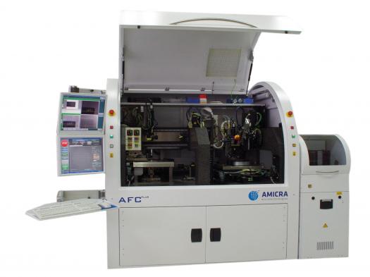
AMICRA Microtechnologies GmbH, German-based vendor of advanced back-end processing equipment, has received a multi-million dollar order from a multinational telecommunications company based in China. The order calls for several of AMICRA's AFC Die Bonder / Flip-Chip Bonder Systems for extremely high-precision bonding offering a placement accuracy of +0.5 µm at 3 Sigma.
AMICRA Managing Director Dr. Johann Weinhaendler welcomed the new order as proof of the company's well known proficiency in the highly demanding and competitive market for advanced processing equipment. "We at AMICRA Microtechnologies are very happy about the new order coming from an important user market of ours. We are looking forward to an excellent customer partnership with a major corporation." The AFC bonders will be used in the packaging of optical devices at the Chinese customer's facility.
The latest large purchase order for the AFC Plus exemplifies AMICRA's earned expertise and continued commitment in providing customers with extraordinary products and engineering services, showing that its specialization on the latest high-precision die-bonder and flip-chip bonders, wafer inking systems, dispense and test systems as well as products for the entire field of microelectronics is paying off big.
AMICRA delivers equipment for active optical cable, fan-out, TSV, TCB, process development, silicon photonics, semiconductor backend, fiber optic, LED, opto-electronics, and MEMS processing.
The ultra-high-precision AFC Plus bonding system was designed as a modular concept for utmost user flexibility and accommodation. AFC Plus realizes a placement accuracy of +0.5 µm at 3 Sigma for die and flip-chip attach. At a cycle time of < 20 sec, it is well suited for processing micro-optic and micro-mechanic components, with eutectic bonding via diode laser or heating plate. AFC Plus provides auto loading of wafers and substrates, wafer mapping, epoxy stamping and dispensing.
Active alignment is provided on request. Post-bond inspection is included; UV curing is featured as an option.
Another of AMICRA's product offerings, introduced in 2010, is the dual-head NOVA Plus Die-attach and Flip-chip Placement system.
NOVA Plus offers high accuracy (+2.5 μm at 3 Sigma) as well as high-speed processing at a very low cycle time of <3 sec. Auto-loading is provided for wafers up to 12 inch (300 mm) diameter and up to 450 mm substrate wafers, with a substrate working area of 500 x 500 mm. With these specs, NOVA Plus is well suited for today's preferred bond processes such as eutectic, epoxy, and laser bonding. Alignment is passive, with active bond force control.
AMICRA, Dr. Weinhaendler says, is committed to continue applying its advanced engineering know-how to keep up with rapidly evolving micro-electronic market demands and providing customers with advanced micro assembly solutions. With its latest die bonder and flip chip bonders AMICRA has evolved and optimized traditional bond processes in the direction of high precision and low cost.


