
Hybrid hope
Backed by IQE, the UK-based Institute of Compound Semiconductors is set to boost III-V on silicon fabrication across Europe. Compound Semiconductor reports.
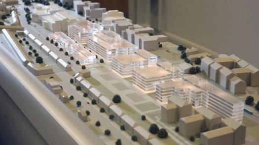
Cardiff University vice chancellor, Colin Riordan, has outlined plans for a £300m campus, including the Institute of Compound Semiconductors, in Cardiff, Wales. [Cardiff University]
In early October this year, the Vice-Chancellor of UK-based Cardiff University, Colin Riordan, unveiled bold plans to build a multi-million pound 'Institute of Compound Semiconductors', that could change the face of materials and device fabrication in the UK.
The new, Wales-based manufacturing facility will focus on fabricating compound semiconductors-on-silicon materials and devices, and could be up and running by late 2016.
IQE is a major partner and as Phil Buckle, Head of Condensed Matter and Photonics at Cardiff, and a key player in the new Institute, puts it: "Drew Nelson the chief executive of IQE is very passionate about this, as is our vice chancellor."
The Institute of Compound Semiconductors (ICS) is part of a grander plan to convert a disused industrial space, in Cardiff, into a cutting-edge tech campus. This would include ICS, a social science park, an innovation centre for start-ups and a research facility to promote commercialisation
But crucially for the semiconductor industry, ICS, would provide manufacturing scale facilities to support an indigenous industry across Europe.
"Right now, if IQE grows an eight inch GaN on silicon wafer, they then have to say to customers, 'if you want to process this, then you've got to go to, say, Singapore'," explains Buckle.
"This is a real problem for the UK and Europe, so the idea here is that our large-scale facilities will cope with this and really pull through our materials into manufacturing markets," he adds.

IQE chief executive, Drew Nelson, is 'very passionate' about the UK-based Institute of Compound Semiconductors [IQE]
The facility will include the main fabrication line for eight inch compound semiconductors-on-silicon. According to Buckle all III-V materials, including GaN, InGaN, InP, and antimonides, are likely to be included with device fabrication ranging from exotic electron spin quantum devices to semiconductor lasers, FETs, and photonic structures.
"For a number of years eight inch [wafer lines] have been the workhorse of silicon foundries and what the compound semiconductor industry now needs is a comparable 'silicon mentality' facility," says Buckle. "Having this facility will also enable high quality research within a highly controlled fabrication plant, bringing reproducible and efficient research based devices through to manufacturing ready technology."
And critically, a small area fabrication line devoted to making research manufacturable and operated by the same engineers as the key fabrication line, is to also be included.
As Buckle points out: "Very often a big barrier for companies is they have to significantly re-engineer research to make it manufacturable. But if the researchers can say, 'with a minimal amount of engineering this can be translated to a large area line', then we have a business."
Off the ground
So the next step is to secure all funds. The University's vice chancellor has promised ICS a significant cut of his £300m innovation budget. Meanwhile, Buckle and colleagues are also busy levering funds from the Welsh Assembly as well as the European Commission's research and innovation pot, Horizon 2020.
And while IQE's input is public knowledge, several other yet-to-be-named companies will also be joining ICS. "We've moved away from the days of large corporations having research laboratories," highlights Buckle.
"And certainly in the compound semiconductor industry, no single company is large enough to sustain pure research without collaboration or the use of shared facilities," he adds.
Buckle is certain that equipment suppliers will also join the new venture; ICS looks set to be a unique facility where the likes of Oxford Instruments may wish to second engineers and trial equipment within a process line.
In the meantime, the researcher expects building work to start within six months, with a fab coming online, at earliest, in two years. And even grander plans are in place, further into the future.
"The long-term goal is for this to stimulate the fifth semiconductor cluster in Europe," he says. "Eindhoven, Dresden, Grenoble and Leuven [imec] are primarily silicon-based but this would be the first cluster based on compound semiconductors."


