
VCSEL visions
As VCSEL manufacturers prepare for industry growth, Anadigics intends to be the first to capture market share. Compound Semiconductor reports.
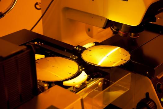
VCSEL ambition: six inch wafers at Anadigics' manufacturing facility in New Jersey, US.
With the VCSEL market poised for rapid growth, semiconductor manufacturers worldwide are ready for action. In March this year, a pan-European consortium including IQE, Philips and ST Microelectronics unveiled bold plans to get VCSEL fabrication ready for volume production in just three years.
Eight months on, Anadigics has joined the VCSEL race offering VCSEL foundry services and having developed the industry's first six inch VCSEL wafer fabrication process. But with production volumes slated for next year, the US-based developer of GaAs semiconductors looks set to lead the pack.
"We have adapted the six inch facility that we've used for our RF processes," says David Cheskis, director of optical products at Anadigics. "We've produced a lot of VCSEL wafers here, customers are sampling products based on these and we believe we will transition to production volumes in the second half of 2015."
As Cheskis points out, the six inch VCSEL line is not a world away from the company's six inch analogue GaAs wafer fab that opened fifteen years ago.

David Cheskis expects VCSEL volume production at Anadigics to start in 2015.
"We work off the same baseline processes with etch tools, position tools and metallisations, and many of the processes have been ported over or adapted from our RF process," he explains. "But we have also needed to implement several different processes that are unique to the VCSEL flow."
"For example, an oxidation furnace has been acquired that was not part of the RF process, and we've developed other rather unique proprietary steps that enable us to fabricate the VCSEL on a six inch [line] using the same basic tool set," he adds.
In addition, Cheskis's team has devised a metal contact process, adapted from that used for RF products and also developed unique six inch VCSEL on-wafer test capabilities.
The Anadigics director is certain manufacturing VCSELs on six inch wafers is going to be crucial to the technology's success. For starters, fabricating VCSELs on the larger GaAs wafers will bring far greater economies of scale than those manufactured within today's three and four inch fabs; cost per square millimetre is lower with more die made per wafer.
And while VCSELs are generally fabricated in a way that may resemble LED or CMOS processing, manufacturing is still relatively slow, and at best, takes place on four inch wafers where process control can be limited and some production steps are still manual.
As the Anadigics director puts it: "The fabs that people use to make three and four inch wafers are very much like laboratories, but our state-of-the-art GaAs facility runs 24 hours a day, seven days a week with the latest operating systems and tools."
"One thing we've learned along the way is that it's really hard to make this transition from three and four inch to six inch," he adds "But we have a lot of experience with this transition, and we've been very aggressive in implementing a VCSEL process on our six inch GaAs facility."

A technician tests six inch VCSELs at the Anadigics test facility in New Jersey.
What's more, Cheskis is also convinced that his company already achieves better process control in its six inch facility compared to a three or four inch fab.
"The same tools as the six inch toolset are used in eight and twelve inch facilities, so we've got a lot of advanced techniques that we can use to control the processes across the wafer," he says. "We've seen very good yields across the wafer for our process and we're getting these again and again."
And while Cheskis won't be drawn on actual yield or device performance figures, he adds: "Just about any VCSEL that can be made on GaAs is something that we have done here."
The right applications.
So which mainstream application will VCSELs find first? Faster datacoms, gesture recognition in smartphones and heat sources in industrial processes are just a few of several up and coming applications that will demand the GaAs VCSEL.
Cheskis believes myriad opportunities are out there with VCSEL manufacturers already busy fulfilling orders for optical communications. He also reckons that if VCSELs fabricated on six inch wafers can hit a similar cost structure to LEDs, then a VCSEL's better performance will drive significant volumes for the technology in, for example, mobile applications.
However, he is also closely watching gesture recognition in mobile phones and reckons this high volume market will really fuel the move from three and four inch to six inch wafers for VCSELs.
"There are many millions of devices for a mobile application that will consume a lot of wafer realty, and I don't think there is enough capacity in the world with existing VCSEL manufacturers [to fulfil demand for mobile applications]," he says. "But because of the time and investment we've made so far, we're ahead of the game and this is an opportunity for us to capitalise on our core competencies in six inch manufacturing."
"We think VCSELs are going to be big and we're very excited about it," he adds.


