Turning To History For High-Temperature Integrated Circuits

BY CARL-MIKAEL ZETTERLING AND LUIGIA LANNI FROM KTH ROYAL INSTITUTE OF TECHNOLOGY, SWEDEN
Imagine for a moment, however, that you rarely had to worry about overheating, thanks to electronics that could operate at really high temperatures, such as those up to 600°C. Armed with this, what would you build?
One obvious area for the deployment of such devices is the monitoring of high-temperature processes taking place in gas turbines, jet engines and combustion chambers, including those used for waste burning.
Although many of today's gas and temperature sensors are capable of handling these temperatures, signals are often too weak, so if an amplifier could be placed right at the source it would deliver a tremendous boost to the signal-to-noise ratio.
There are also applications where silicon ICs are currently operating at their very limit, and an alternative circuit made of a different material and capable of higher operating temperatures would be highly valued. That is the case for oil, gas and geothermal drilling operations, which currently rely on commercial, high-temperature silicon-on-insulator (SOI) circuits recommended for use up to 225°C. When deployed in these applications, premature failures are very costly − and a rule of thumb says that an extension of temperature by only 10°C halves the mean-time-to-failure.
What's needed is a semiconductor material that is capable of forming circuits operating at much higher temperatures. There are several candidates for this, but the most promising by far is SiC. Great strides have already been made with this wide bandgap semiconductor: It has led to commercial discrete devices capable of handling 1700 V or more, and research has shown operation at up to 600°C. However, more work is needed to improve this technology, including the development of ICs, capacitors and packaging that can operate at extreme temperatures.
Driving efforts in this direction is our team at KTH Royal Institute of Technology, which is based in Stockholm, Sweden. We have developed a variety of analogue and digital circuits that can operate at very high temperatures.
We are by no means the first research team that has turned to SiC to realise circuits capable of operating at extreme temperatures. One of the pioneers of this field is a group at NASA, which demonstrated SiC integrated JFET circuits of low complexity more than 20 years ago. Although this class of transistor can operate over an extended temperature range, it is tricky using it as the building block for designing ICs, due to a combination of difficulties associated with threshold voltage matching, variations in threshold voltage over temperature and a limited selection of circuit topologies.
Another trailblazer of SiC circuits is James Cooper from Purdue University. He leads a group that in 1993 demonstrated SiC NMOS and CMOS ICs that could operate at 300°C.
Following these efforts, the operating temperature of SiC ICs has climbed over the intervening years. In 2014 MOSFET technology enabled the construction of circuits operating at 500°C, showing the capability of NMOS and CMOS ICs. And as is the case for silicon and SOI, it is the gate dielectric, rather than the semiconductor material itself, that limits reliability.
High gate fields of 3 MV/cm or more are needed to extract sufficient current from the SiC MOSFETs, and this exerts more strain on the device, accelerating failure.
Another downside of the SiC MOSFET is the lack of a simple production process. If ion implantation is used, an annealing step is required at 1600°C, and this high temperature makes self-alignment of the source and the drain to the gate incredibly challenging. Consequently, to date all SiC MOSFETs are made without self-alignment, typically limiting integration to a gate length of 1 mm.

Back to the future
To find the best way forward we have delved into the past, studying a semiconductor technology from the 1960s: The bipolar integrated circuit formed in silicon. This technology ruled the roost until silicon CMOS reached a sufficiently high level of reliability that allowed it to dominate the integrated circuit, just like it does today.
Should you open a recently written microelectronics textbook, you'll see that the focus is on the CMOS IC. But if you can get your hands on a 1960s textbook, you will find circuit topologies for every function formed from the bipolar junction transistor (BJT).
One of the great strengths of the BJT is that its threshold voltage does not vary with temperature. Although that's unfortunately not the case for built-in voltage, which drops by around 2 mV/°C, this dependency can be exploited, allowing the creation of bandgap
voltage reference circuits that counteract the influence from temperature variations "“ this is the approach that is adopted in precision analogue-to-digital converters. What's more, we have shown that discrete BJTs and entire ICs can be realized without any ion implantation, circumventing the need to perform high-temperature annealing, which causes defects and ultimately impacts performance and reliability.
We have been developing our SiC BJT technology in our own university cleanrooms for more than a decade. Milestones in this project include the development in 2005 of n-p-n BJTs capable of handling up to 3 kV. Since then we have refined process and device, with the peak operating voltage of our BJTs increasing to 6 kV.
There are some key differences between the design of a high-voltage switch and an IC technology. With a switch, current is conducted from the front side to the backside of the wafer, with the collector region in the substrate (see Figure 1).
In comparison, for an IC technology, the BJTs must be isolated from one another, and all contacts made to the front side. We insert an extra p-type isolation layer to address this need, and have turned to thinner epitaxial layers, due to the targeting of lower voltages.
Other key building blocks for the IC are the resistor and the capacitor. With our technology, integrated resistors can be implemented in emitter, base and collector layers by accounting for the expected sheet resistance and specific contact resistance of the selected layer. Note that typical room temperature sheet resistance values for tested epitaxial structures are between 100 and
200 Ω/square for emitter and collector layers, while for the base layer, resistance ranges from 20 to 80 kΩ/square, depending on doping concentration. It is possible to form capacitors between the emitter layer and metal layer, but they are limited to tens of pF to prevent them from either taking up too much area or introducing too large a series resistance.
Starting from scratch
As this is an in-house technology, there is no design kit. Instead, everything has had to be developed, starting from the epitaxial structure and layout of the BJTs. Following this, we carried out physical device simulation that accounts for the doping and thickness of all active regions, and have also undertaken the development of specific process steps and circuit level models for the BJT, which are a pre-requisite for circuit design.

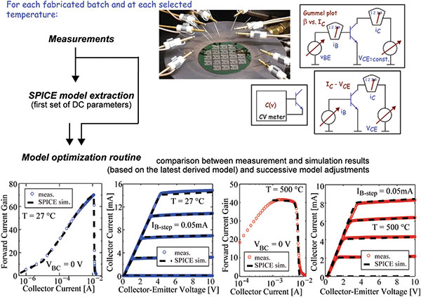
Figure 2. SPICE models are continuously improved, using measurements from each batch at several different temperatures. However, it is only mainly DC parameters that have been fully characterised, so AC performance can only be measured after completion.
A key part of this work has been the development of a SiC etching process. This has had to realise adequate uniformity across an entire SiC wafer, initially 50 mm in diameter and now 100 mm. We have found that the first etch that isolates the emitters is critical "“ remove too much material and the base layer becomes too thin (or even disappears), leading to increased extrinsic base resistance. Another challenge results from the mesa-etching that takes place on a wafer containing the entire epitaxial stack, but has not been subject to ion implantation. After etching, steps between adjacent regions on the surface can be as high as 1 mm, making it challenging to add interconnects, even if they only involve one metal layer.
Before we fabricated the first batch of ICs, we developed BJT SPICE models that were at least adequate for DC simulation by drawing on measurements on our existing high-voltage BJTs. Unfortunately, temperature variation models in SPICE are not suitable for SiC BJTs, so separate models had to be obtained for different temperatures. Consequently, after fabrication of the first IC batch, and for each successive batch, new BJT SPICE models have been extracted at discrete temperatures in the range 27°C to 500°C (see Figure 2 for the used methodology and models extracted at two temperatures).
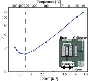
Since we made our first batch, our biggest concern has been the impact of temperature variation on circuit design. Unfortunately, changes in temperature cause many problems: They impact current gain, which can fall by 50 percent when the transistor temperature rises from room temperature to 300°C (see Figure 5); and they are also behind changes in the sheet resistance of the SiC epitaxial layers and, therefore, the resistance of integrated resistors. The good news, however, is that although large variations in the resistance are expected for temperature changes of hundreds of degrees, it is possible to stabilise the DC operating point of bipolar analogue circuits with junction cancellation techniques and resistor ratios, rather than absolute values.
We are delighted to report that our ICs worked since the first batch. We began by making individual BJTs and digital integrated circuits using emitter-coupled logic (ECL), another 1960s technology. To assess the performance of these devices, we carried out on-wafer probing on a temperature-controlled stage that enabled testing up to 300°C. Due to the higher bandgap of SiC than silicon, the SiC ECL needs to be fed with -15 V, compared with -5.2 V for the silicon equivalent.

Figure 3. Manual layout of transistors and resistors is time-consuming when only one metal layer is available. Resistors have to be used sometimes to cross connections. Capacitors consume much area and are used sparingly.
The current gain of these HBTs diminishes with temperature, falling from 40 at room temperature to 20 at 200-300°C. However, these digital circuits are sturdy enough to successfully operate at up to 500°C and even 600°C, as we have shown for similar gates fabricated in later batches.
To learn as much as possible from these batches, they are used to assess a variety of analogue circuits, including: several different operational amplifiers (one was covered in detail in Compound Semiconductor 6 65 (2014)), Schmitt triggers, BJT drivers, digital-to-analogue converters and even a sigma delta modulator. All these elements can work at up to 500 °C.
As these circuit have just been produced for demonstration purposes, it is no surprise that they deliver an inferior performance at room temperature to those made from silicon CMOS. However, crank the temperature up to in excess of 300°C, and there is simply no alternative to the SiC IC.
Inspect our ICs in detail, and you'll also find that the level of integration is reminiscent of the 1960s: 100 transistors and 100 resistors are typical counts for the largest digital and analogue demonstrators we have made. We have also constructed smaller BJTs with higher current gain, and we have developed two-layer metallisation that enables our technology to be suitable for making many analogue circuits, including complete analogue-to-digital converters.
Another recent development is that of a lateral p-n-p BJT formed with the same technology, aside from the addition of one mask layer. This opens the door to the creation of even more textbook circuits in our IC technology.
However, for digital circuits in ECL, scaled BJTs imply lower currents but higher resistor values and thereby larger resistors, so it is not easy to see a way forward to very highly integrated digital circuits.


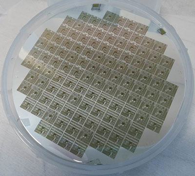
Figure 4. The finished circuit corresponding to the layout in Figure 3 is part of a test chip of 7 mm by 7 mm, and above that is the full 100 mm wafer with several different designs.
Questions that we are often asked are what are the temperature limits for our devices and circuits, and what level of reliability can be expected at 600°C. Although some digital circuits have been shown to work at 600°C, the aluminium-based metallisation is not suitable for such extreme temperatures. That's because the melting point of aluminium is only just above this, at 660°C, while the metal diffusion barrier, a TiW layer, is unstable above 500°C.
An attractive alternative is platinum, and we have used this for interconnects in some test circuits. Its downside is that patterning is much more challenging, and this has led us to use lift-off rather than dry etching.
We are yet to perform complete reliability testing, because this will require packaged devices, rather than on-wafer contacting with probes. Our hot-stage on a probe station is also unsuitable for scrutinising reliability, because it is not designed for 500 hours of operation, and the needle contacts are not reliable for repeated probing.
It also makes sense to introduce hermetic packaging of the ICs, a step that would surely extend lifetime. In short, reliability testing is not relevant until our SiC technology is fully developed, including relevant ICs with final passivation layers. Overarching all of these practical difficulties is the need to find testing procedures for operating temperatures that are far higher than those employed for most of today's accelerated testing. Figure 4. The finished circuit corresponding to the layout in Figure 3 is part of a test chip of 7 mm by 7 mm, and above that is the full 100 mm wafer with several different designs.
Often the best way to accelerate the capability of a technology is to take on a tough but achievable target. We have adopted this strategy, trying to demonstrate all electronics needed for a Venus lander. The surface temperature of this planet, the second from the sun, is around 460°C, so there will be no human accompaniment on any mission, and all data collection and transmission will have to be automatic. To do this will require sensors, amplifiers, ADCs, a CPU, memory, a radio transceiver and power supply.
Although we don't expect to become rich from designing electronics for an exploration of Venus, we are sure that the developed high-temperature SiC electronics will find several terrestrial applications, such as aerospace, combustion monitoring, and drilling operations. This is bound to be a hot topic in the future.

Figure 5. The n-p-n BJT current gain varies considerably over the entire temperature range, so circuit designers have to take this into account. A different probe station was used for characterisation down to -40°C.

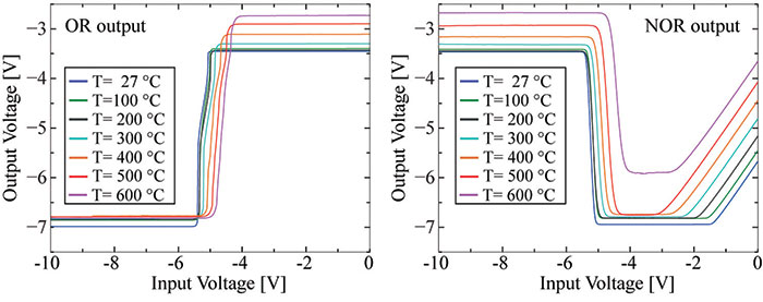
Figure 7. Transfer characteristics of a digital ECL OR-NOR gate (NOR output shown). Noise margins can be extracted from these curves, and this specific design achieves almost 1.5 V noise margin over the entire temperature range.
Further reading
The research publications resulting from the HOTSiC project are provided from the home page www.hotsic.se More information
on the Venus project can be found at www.workingonvenus.se


